 Mitsuru Yamada
1-1. Simple discrete op-amp
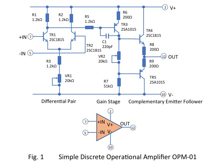
The inside of a commercially available op-amp consists of many monolithic transistors, but in this case, I decided on a circuit with only five transistors to make the operation as simple as possible as shown in Fig.1. The transistors used general-purpose NPN and PNP complementary pair transistors. I thought I had achieved at this circuit configuration by my own ingenuity, but when I searched the net again now, I found several similar circuits published. I guess the limitation of five transistors means that anyone can reach the same solution.
1-2. Differential pair
Shown in Fig.1, the differential pair consists of two transistors TR1 and TR2. Offset adjustment of the entire operational amplifier is done by VR1. This VR1 needs to be a multi-turn type. In commercial operational amplifiers, this is not necessary because each individual unit is laser-trimmed.
1-3. Gain stage
The gain stage consists only of a transistor TR3. The capacitor C1 is for phase compensation and is set to a large value for stability. If C1 is not used, a frequency characteristic of GB product = 4MHz can be obtained, but it may cause micro oscillation.
1-4. Complementary emitter follower
The output stage of this op-amp is an ordinary complementary emitter follower by TR4 and TR5. This stage is no voltage gain but has current boosting. The VR2 is used to experiment with different biases to see the crossover distortion.
1-5. Results
Figure 2 shows an example of a non-inverting amplifier configuration and Fig. 2-1 shows input/output waveforms of the measurement . The oscilloscope's upper signal is 10kHz 280mVp-p sine wave input signal and the lower signal is the output signal. The measured resistances R51 = 5.02k ohm and R52 = 50.4k ohm gave a theoretical gain of x11.04, while the measured gain was x10.96 with a gain error of 0.7%. This was good enough for learning purposes.
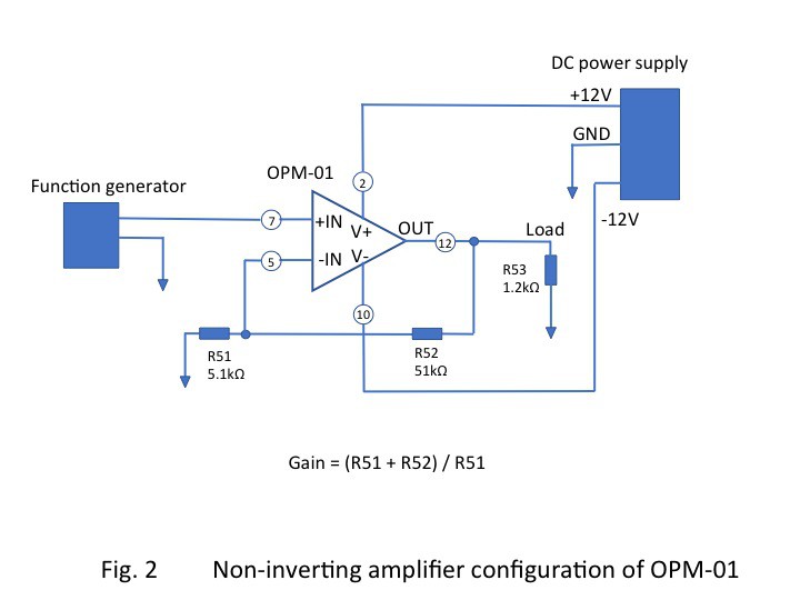
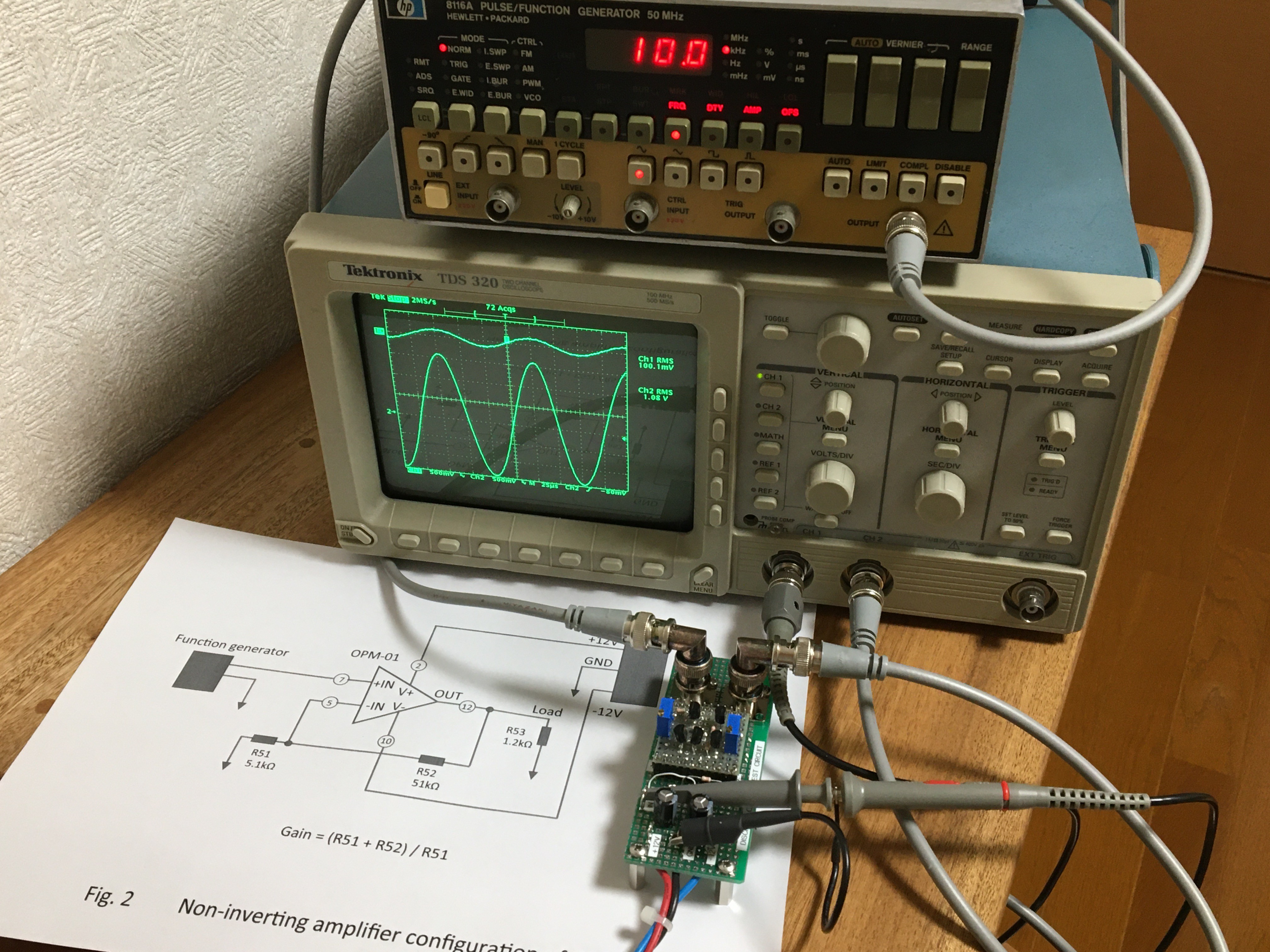
Fig. 2-1 Measurement of input/output waveforms of non-inverting amplifier configuration
Following video shows an open loop drift,
(00:00) if TR1 and TR2 are thermally uncoupled and the temperature changes by touching either of them, the output voltage can be seen to drift.
(01:08) If TR1 and TR2 are subjected to the same changes, the output drift will cancel out and you will feel the differential circuit in action.
Adjusting VR2 to zero ohms will cause TR4 and TR5 to operate in class B, resulting in crossover distortion; adjusting VR2 to around 5 k ohms will increase the bias voltage of TR4 and TR5, eliminating crossover distortion.
2. Audio power amplifier
Figure 3 shows a modification to a power operational amplifier. With the emitter follower in Darlington configuration TR6 and TR7 attached, it can drive 0.35A DC for an 8 ohms load. The stereo audio power amplifier shown in Fig. 4 is built with the power op amps. The output power is 1 watt, so I can listen to sound sources such as CD players through the speakers.
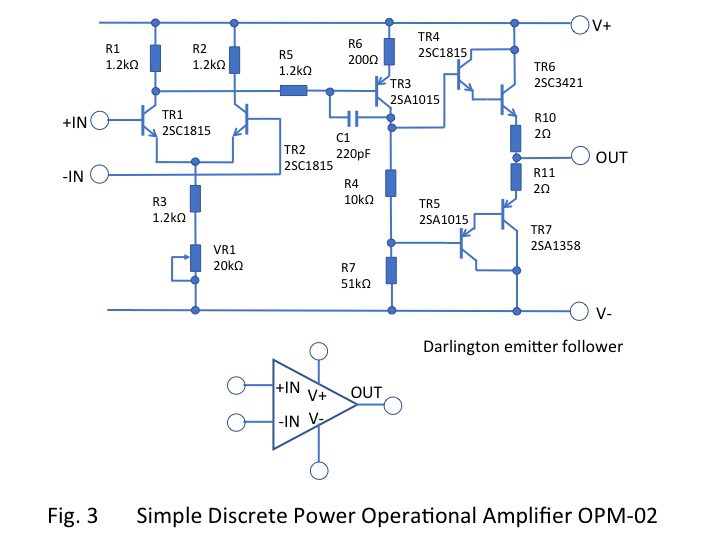
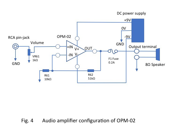
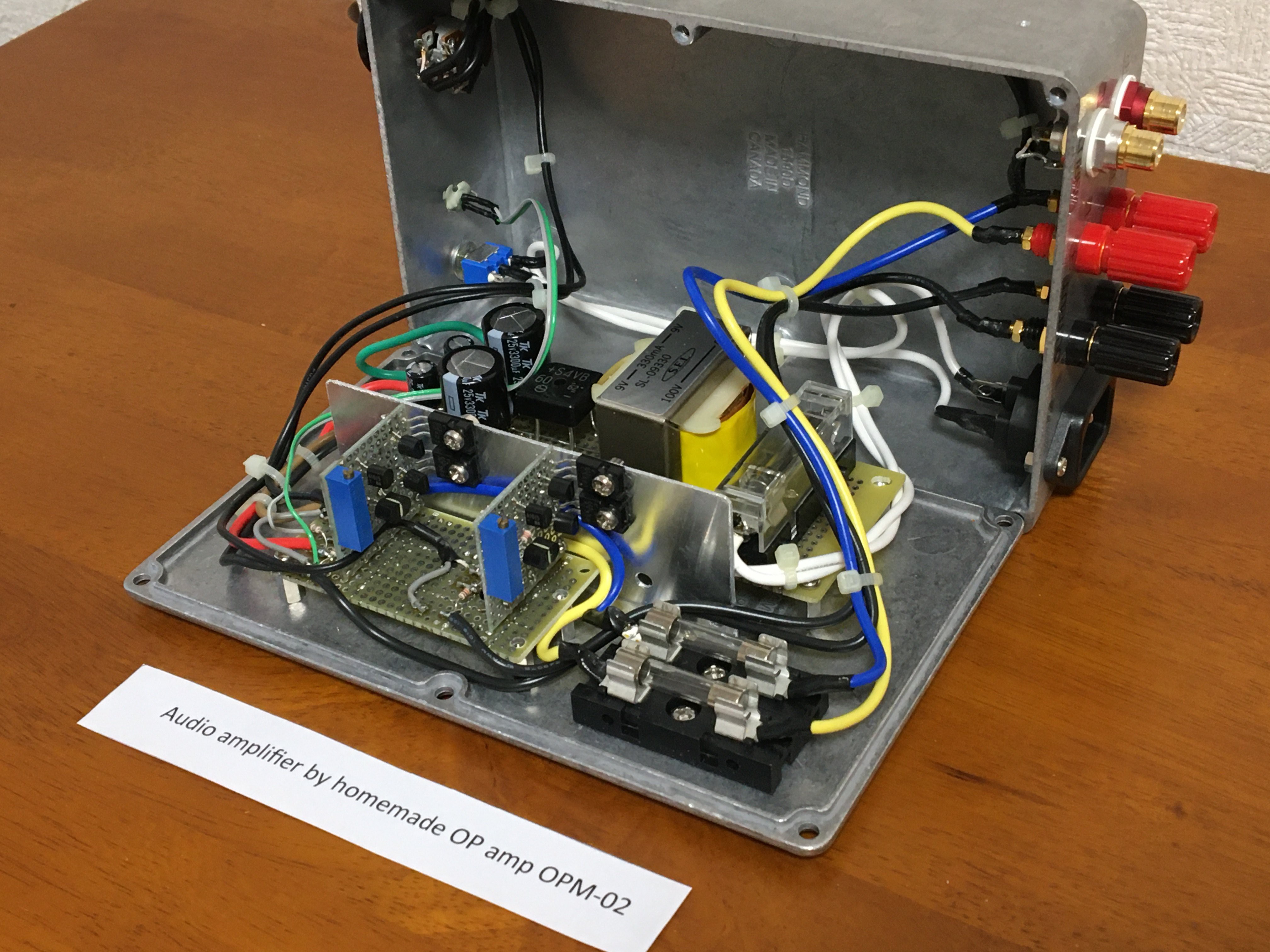
Fig. 4-1. Audio amplifier by using the homemade power operational amplifier OPM-02


 mit41301
 Boolean90
 Nick Sayer
 mircemk
Any comment or advice about the Gain stage ? I think that some circuits use a Darlington pair instead of one.