Close
0%
0%

Apollo Guidance Computer

A running hardware implementation of the AGC, block II using TTL chips.

Similar projects worth following
This project includes building a hardware based simultor to understand how the AGC works at the hardware level and then wiring together TTL chips to run the actual AGC assembly code.

This project extends the work of Ronald Burkey who created an extensive collection of NASA documents, original source code, an assembler and a software based simulator plus the work of John Pultorak who created a physical implementation of the AGC Block I computer using TTL chips. There are other AGC Block II projects using either VHDL or 3-input XOR chips. As far I as I can tell, this is the only project to implement an AGC Block II using TTL chips.

Why build a replica of the Apollo Guidance Computer? I have always wanted to build a computer based on TTL chips ever since that college lab course that taught the use of TTL chips. During my career as a software developer I was fortunate enough to work on a project that used a real time operating system where I was able to understand the intricacies of the operating system. I wrote device drivers for hardware boards that were created in house as well as the infrastructure add-ons. That was my favorite work project. Modern software developers have become so abstracted from the hardware and operating systems that their code is typically platform independent.

I want to understand a historic computer's architecture, both hardware and software, and what better computer than the Apollo Guidance Computer. The AGC has a serious coolness factor because it landed men on the moon and it was the first computer to use integrated circuit chips, thus bridging the gap between computers made from vacuum tubes and modern computers. The original Block I AGC was built using 4,700 single 3-input NOR gate chips. NASA pushed the manufacturers to improve the integrated circuit technology and reliability by creating the first flat pack chip. The Block II version of the AGC used these flat chips that contained two 3-input NOR gates. The Block II version was built from 2826 dual 3-input NOR gates (RTL chips) along with 3325 diodes and core memory. NOR gates were used because they are the “universal” gate from which all other logic gates can be derived. It was cheaper and quicker to throw all the time and money into developing one reliable chip at the cost of having to use more chips.

The AGC was designed and built by MIT in the early 1960s. The only small size computers of the time were developed to guide ballistic missiles. MIT was designing guidance control systems for the Polaris submarine launched missile. The Block I version of the AGC had 24K of ROM, 1K of RAM and 11 instructions. The Block II version had 36K of ROM, 2K of RAM and 34 instructions. Block II was based on the Block I architecture. Both were 16-bit computers with a clock speed of 1.024 MHz.

At the time there was no light weight, simplistic computer interface technology appropriate for a space capsule. The astronauts, who were test pilots, wanted gauges and dials as they would find in an airplane. The AGC used a simple keyboard and numeric displays. This calculator style interface was the first of its kind. The Block I version only supported the Command Module and flew the unmanned missions up through Apollo 6 where the Block II flew all the manned missions. The Block II upgrade was required as it also needed to fly the Lunar Module.

The AGC was designed using technology that did not exist at that time. By the end of the Apollo era, computer technology had progressed to the point that the AGC was obsolete. Manufacturers had gone on to produce the TTL series of chips that are still available today. As with most government contracts, there was not enough time or money to completely redesign the AGC with this newer technology.

The AGC solved two very difficult problems for aircraft that did not exist or were in their infancy, a digital autopilot and digital fly-by-wire. Autopilots of the time were analog devices that were large and heavy with limited capabilities. The X-15 project was just starting to introduce this technology. After the Apollo missions were complete in 1975, a surplus AGC was retrofitted into a F-8 Crusader fighter jet to be the first fly-by-wire aircraft. The other ground breaking feature was the incorporation of the newly developed Kalman filter algorithm. This was one of the first applications of the Kalman filter which is now ubiquitous in spacecraft and missile implementations.

Add on top of all that the fact that this computer and its software had to execute flawlessly, yet could not be fully tested ahead of time before actually landing on...

Read more »
  • Processing Sub-System

    wglasford07/07/2022 at 12:34 0 comments

    I have created an initial set of schematics for this sub-system, but have not yet started wiring it up.

    Here are design notes that help understand the schematics.

    Central Registers: The Central Registers module implement the A, L, Q and Z registers along with implementing the ANDing, ORing and XORing of the A register with the Channel bus. The four central registers have numerous sources of data and various control pulses that perform specific functions. This is all straight forward logic.

    The Z register has logic to perform the Z15 and Z16 command pulses. These pulses set the Z register to 040000 and 0100000 respectively.

    The WALS command pulse is not simplistic.

    Part of the central registers is the logic read from and write to the channel bus. This logic involves ANDing, ORing and XORing the contents of the A register with the bus data. To simplify the design and the chip count, four 74LS181 ALU chips are used. These chips have a 4-bit mode select. The Mode Control is set high to inhibit internal carries. The A data is set to the contents of the A register while the B data is set to the contents of the channel bus. The write to the channel bus is either a straight pass through, A anded with the channel data or A ored with the channel data. The read from the channel bus also can perform an xor of the data. Note that the instruction indicators are logic low. The following table defines the operations and the mode control values.

    FunctionS0S1S2S3
    WRITELHLH
    WANDHHLH
    WORLHHH
    READLHLH
    RANDHHLH
    RORLHHH
    RXORLHHL

    WS0 = !WAND

    WS2 = !WOR

    WS1 = WS3 = High

    RS0 = !RAND

    RS1 = High

    RS2 = !ROR + !RXOR

    RS3 = !READ + !RAND + !ROR

    Arithmetic Logic Unit: This module is the most complex of the modules requiring the most design effort. The X, Y, U and B registers are implement in this module. There is also a pseudo C register which is simply the 1's compliment of the B register. The X and Y registers have numerous control pulses to load them with various values. The X and Y registers feed four 4-bit adder chips used to add their values. The output of the adders is contained in the U register.

    The U register's bit 16 is either the output of the ALUs or the sign bit (bit 15) extended into bit 16 if RUS is asserted.

    The end-around carry bit logic is rather complex as the multiply uses 2's compliment arithmetic where everything else in the computer uses 1's compliment arithmetic. The sub-sequences can disable the end-around carry. The end-around carry is disabled during a multiply using the NEACON and NEACOF. This value is stored in a 1-bit register.

    The X register has five control pulses that generate six outputs. These include B15X which generates an octal 060000, PONEX which generates an octal 000001, PTWOX which generates an octal 000002, a combination of PONEX and PTWOX which generates an octal 000003, MONEX which generates an octal 177776 and ZERO which zeros the X register. A bit table in MSB first format is as follows.

    PulsesBit Pattern
    B15X0100000000000000
    PONEX0000000000000001
    PTWOX0000000000000010
    P1X + P2X0000000000000011
    MONEX1111111111111110
    ZERO0000000000000000

    The only bits with any complexity are bits 1 and 2. Their equations are as follows.

    1 = !M1X + (P1X + P1X P2X)

    2 = M1X + (P2X + P1X P2X)

    The U and B registers feed four 4-bit ALU chips that can perform a number of combinational logic sequences. The output of the ALU chips go directly to the Write Bus. The pulses that drive the ALU logic include the RB, RC and RU. The following equations are required and numbered for reference. WB is the Write Bus.

    if RC then
    
    	if RA then WB = A + B  (A in WB) 	: 0
    
    	else WB = B				: 1
    
    if RB then WB = B				: 2
    
    if RU then
    
    	if RC then WB = B + U			: 3
    
    	else if RB then WB = B + U		: 4
    
    	else WB = U				: 5
    

    Equation 0 is implemented separately due to the fact that the A value is contained within the Write Bus. The ALU chip has four control bits. The following table identifies the control bits required to implement the equations.

    Equation...
    Read more »

  • Control Sub-System

    wglasford07/07/2022 at 12:31 0 comments

    I have drawn initial schematics for this sub-system, but have not started wiring it up.

    Here are design notes that help understand the schematics.

    Clock: At the heart of the Clock module is a 4 MHz crystal that is divided into four non-overlapping 1 MHz clock signals; CLK1, CLK2, CLK3 and CLK4. This allows the read data to be placed on the bus before the write signals latch the data into the registers. The clock signal can be replaced by a 555 monostable multi-vibrator chip with a variable resistor to provide a slower, variable clock for debugging purposes. The output of these two sources are used to create the two clock pulses.

    The two clock signals are generated using two J-K flip-flops. The following table shows the states of the two flip-flops and their meaning. The first flip-flop (FFA) has its J & K inputs tied high, putting that flip-flop into a toggle mode. The Q output of the first flip-flop feeds the J/K input of the second flip-flop (FFB). This puts the second flip-flop into a hold/toggle mode. The Q and !Q outputs of both flip-flops are ANDed together as follows.

    FFA QFFA !QFFB QFFB !QSignal
    XXCLK1
    XXCLK2
    XXCLK3
    XXCLK4

    Scalar: The Scalar module successively divides the first clock pulse in half using six 4-bit counters. Three clock pulses are pulled out of the scalar. The F10 output is a 100 Hz clock pulse used to drive the time counters. The F13 output is a 12.5 Hz clock pulse used in the TPG module. The F17 output is a 0.78125 Hz clock pulse used in the TPG module. These can also be manually generated for debug purposes. Note that a 2.048 mHz crystal is not available, so a 2.0 mHz crystal will be used. This means the real time clock will not be exactly accurate, but close enough.

    The first 4-bit counter divides the 1 MHz clock pulse by ten, resulting in a 51.2 kHz clock pulse. The next five 4-bit counters count down and therefore divide the 51.2 pulse by two.

    Timing Pulse Generator: This module is a state machine used to sequence through the timing pulses that make up a memory cycle. There are 12 timing pulses plus two additional pulses to perform startup and two pulses to perform debugging. These 16 timing pulses are cycled via a 4-bit counter. Most state changes occur via the clock 1 pulse unless the system is being debugged. In this case there are state change equations that drive the state machine.

    The timing pulse generator is driven by CLK1 which is delayed so the write bus can be written to before the TPG changes state.

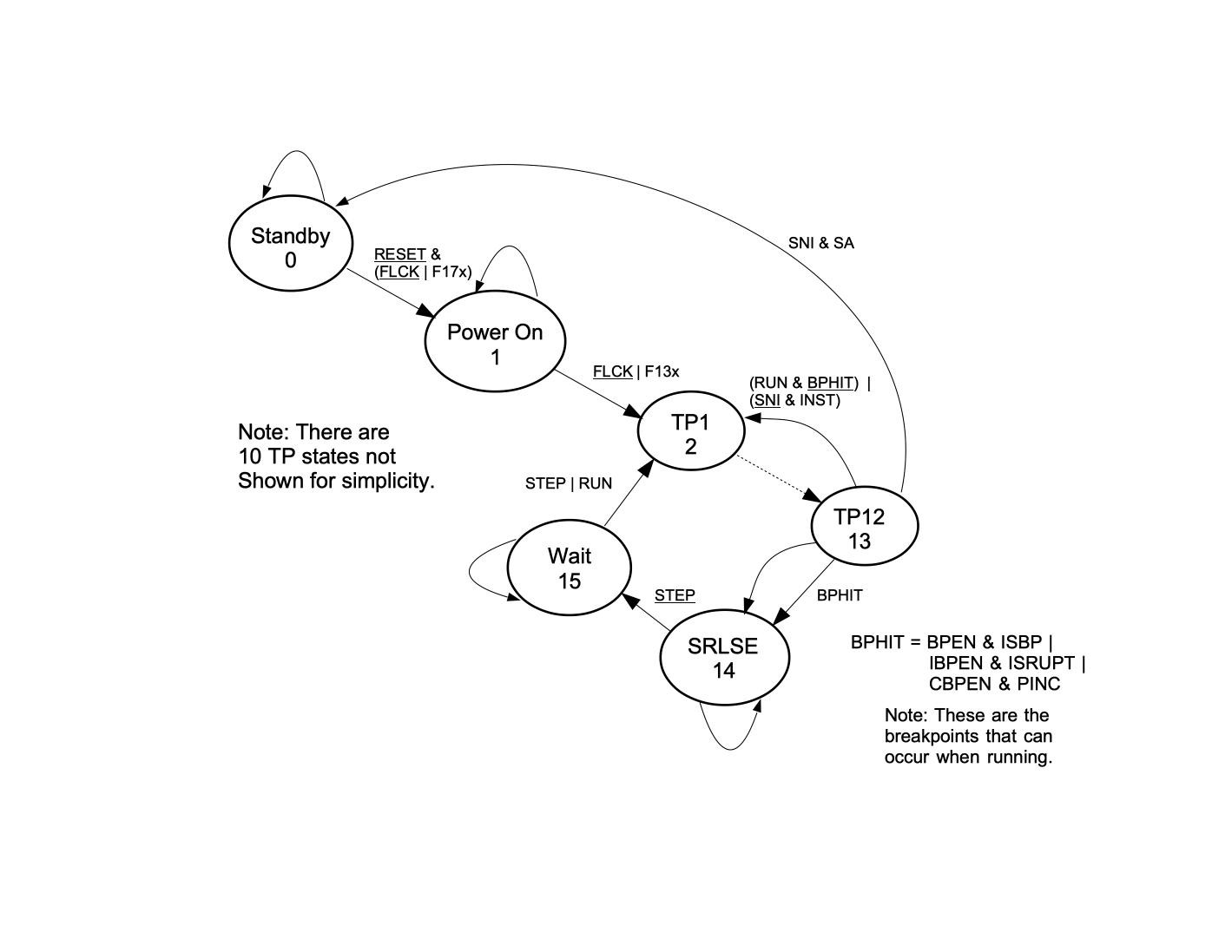
    There are a number of state changes that are numbered and listed below. Note that moving from TP1 through TP12 is performed via the counter which free runs if the CET input is 1.

    From StateTo StateNumberEquation
    STBYPWRONTPG_0!RESET * (!FCLK + F17)
    PWRONTP1TPG_1!FCLK + F13
    TP12TP1TPG_2(RUN * !BPHIT) + (!SNI * INST)
    TP12STBYTPG_3SNI + SA
    TP12SRLSETPG_4BPHIT = (BPEN * ISBP) + (IBPEN * ISRUPT) + (CBPEN * PINC)
    SRLSEWAITTPG_5!STEP
    WAITTP1TPG_6STEP + RUN

    The logic driving this implementation depends heavily on the 74LS161 counter chip. There are two inputs that drive the logic. The first one is the PE or NPE pin. When set low, data is loaded from D0-D3. This data sets the next state to TP1. When NPE is set high, the logic is controlled by the CET pin. The CET pin, when set low operations are put on hold. When high, the chip counts once per clock pulse. The following table shows each state and what these pins need to be to move to the next state.

    StateCurrent DCBANext DCBA012345678NPECETComment
    STBY0 0 0 00 0 0 00xxxxxxxx10Goto STBY
    ..0 0 0 11xxxxxxxx11Goto PWON
    PWON0 0 0 10 0 0 1x0xxxxxxx10Goto PWON
    ..0 0 1 0x1xxxxxxx11Goto TP1
    TP10 0 1 00 0 1 1xxxxxxxxx11Goto TP2
    TP20 0 1 10 1 0 0xxxxxxxxx11Goto TP3
    TP30 1 0 00 1 0 1xxxxxxxxx11Goto TP4
    TP40 1 0 10 1 1 0xxxxxxxxx11Goto TP5
    TP50 1 1 00 1 1 1xxxxxxxxx11Goto TP6
    TP60 1 1 11 0 0 0xxxxxxxxx11Goto TP7
    TP71 0 0 01 0 0 1xxxxxxxxx11Goto TP8
    TP81 0 0 11 0 1 0xxxxxxxxx11Goto TP9
    TP91 0 1 01 0 1 1xxxxxxxxx11Goto TP10
    TP101 0 1 11 1 0 0xxxxxxxxx11Goto TP11
    TP111 1...
    Read more »

  • Understanding the computer - Part 2

    wglasford07/07/2022 at 12:18 0 comments

    Here are additional details you need to understand including the Control Pulse Matrix and the instructions.

    The control pulses are the heart of the system. Each instruction has a sequence of control lines that are activated to cause data to flow through the system. Some of the control pulses have a control number in the control number column. These numbers came from the R-700 documentation. Through testing it was discovered there are a few minor errors in the matrix. I found another version that had the correct control pulses. These errors were in the multiply and divide instructions.

    The following table is a combination of design and implementation. It lists each control pulse, where it originates and terminates on the hardware diagrams and what function is performed. The hardware diagram names are sub-system followed by module followed by sub-module. The Active State column can have a value of Low or High meaning the control pulse is active low or high, or values of Pulse meaning it is a pulse such as a clock pulse or a value of Bit meaning the value represents a bit value. Most of the control pulses are active low because many of the TTL chip inputs that are controlled are active low. That and many more of the TTL chips are active low logic. The few control pulses that are active high were chosen to be because that resulted in fewer chips required.  Just an FYI, this table formats better on my GitHub wiki page.

    Control LineOriginDestinationPurposeCntl #Active State
    A2XCTL-CPM-APROC-CRG-AREG, PROC-ALUCopy A1-16 into X1-16 by private line (i.e. not through WL).1Low
    B15XCTL-CPM-APROC-ALUSet bit 15 of X to 12Low
    BR1CTL-SEQCTL-CPM-ABR1 staten/aLow
    BR2CTL-SEQCTL-CPM-ABR2 staten/aLow
    CICTL-CPM-APROC-ALUSet carry in bit into CI register. Adds 1 to adder value.3Low
    CLXCCTL-CPM-APROC-ALUClear X register if BR1=0. Used in Divide.4Low
    CLISQCTL-CPM-CCTL-SEQClear the SNI bitn/aLow
    CLK1CTL-CLKAll1 MHz Clockn/aPulse
    CLK2CTL-CLKAll1 MHz Clockn/aPulse
    CLK3CTL-CLKAll1 MHz Clockn/aPulse
    CLK4CTL-CLKAll1 MHz Clockn/aPulse
    CLRPCTL-CPM-CMEM-INTClear RpCell registern/aLow
    DCDSUBCTL-CPM-CCTL-SEQDecode Sub-sequencen/aLow
    DISPCTL-CPM-BDSKY-DSPWrite to Channel 10n/aLow
    DVSTCTL-CPM-ACTL-SEQCause Divide staging by complimenting the next higher bit position. Sequence: 0, 1, 3, 7, 6, 4.5Low
    DOTP1CTL-SEQCTL-CPM-CDo TP1 commandsn/aLow
    DOTP4CTL-SEQCTL-CPM-CDo TP4 commandsn/aLow
    DOTP6CTL-SEQCTL-CPM-CDo TP6 commandsn/aLow
    DOTP7CTL-SEQCTL-CPM-CDo TP7 commandsn/aLow
    DOTP10CTL-SEQCTL-CPM-CDo TP10 commandsn/aLow
    DOTP12CTL-SEQCTL-CPM-CDo TP12 commandsn/aLow
    EQU3MEM-MBFCTL-CPM-BInstruction address = 3n/aLow
    EQU4MEM-MBFCTL-CPM-BInstruction address = 4n/aLow
    EQU6MEM-MBFCTL-CPM-BInstruction address = 6n/aLow
    EQU17MEM-ADRCTL-SEQInst. address = 17n/aLow
    EXAMNXTMEM-ADR_SMEM-ADR-MDEExamine next key pressedn/aLow
    EXTCTL-CPM-A, CTL-CPM-BCTL-SEQ-SEQBSet the extend bit.6Low
    EXTENDCTL-SEQ-SEQBCTL-CPM-C, CTL-CPM-A, CTL-SEQ>td >n/aBit
    F10XCTL-SCLMEM-CTR-CTL100 Hz timeoutn/aLow
    F13XCTL-SCLCTL-TPG12.5 Hz timeoutn/aLow
    F17XCTL-SCLCTL-TPG0.78125 Hz timeoutn/aLow
    FCLKCTL-MONMEM-ADR-MDEClock Moden/aLow
    GENRSTCTL-MONAllGeneral Resetn/aLow
    G1MEM-MBFPROC-CRG-AREGG reg bit 1 valuen/aBit
    G16MEM-MBFPROC-CRG-AREGG reg bit 16 valuen/aBit
    G2LSCTL-CPM-APROC-CRG-LREG, MEM-MBF-GMBCopy G16,15-4,1 into L16,12-1 and X157Low
    GETBPCTL-TPGMEM-ADR-ATS, MEM-ADR-CTLGet Breakpoint Addressn/aLow
    GMZMEM-MBF-GMBCTL-SEQ-SEQAG reg. is all zerosn/aLow
    GPMEM-EFMMEM-PARGenerate Parityn/aLow
    GTR7MEM-ADR-CTLCTL-CPM-BAddress is > 07n/aLow
    GTR1777MEM-ADR-CTLCTL-CPM-B, MEM-EFMAddress is > 01777n/aLow
    INDCCTL-CPM-BDSKY-DSPWrite to channel 11n/aLow
    INHINTCTL-CPM-BMEM-INTExecute INHINT commandn/aLow
    INTRCTL-CPM-CCTL-SEQPerform Interrupt (RUPT)n/aLow
    IRQMEM-INTCTL-CPM-CInterrupt requestedn/aLow
    ISBPMEM-ADR-CTLCTL-TPG>td >n/aLow
    ISRUPTMEM-INTCTL-TPGIs an interrupt pending?n/aLow
    KB_STRDSKY-KBDMEM-INTKey Strobe, data is latchedn/aLow
    KBD1CTL-CPM-BDSKY-KBDRead Channel 15n/aLow
    KRPTCTL-CPM-AMEM-INTReset the current RUPT priority (cell).8Low
    L1PROC-CRG-LREGCTL-CPM-BL register...
    Read more »

  • Memory Sub-System

    wglasford07/06/2022 at 23:54 0 comments

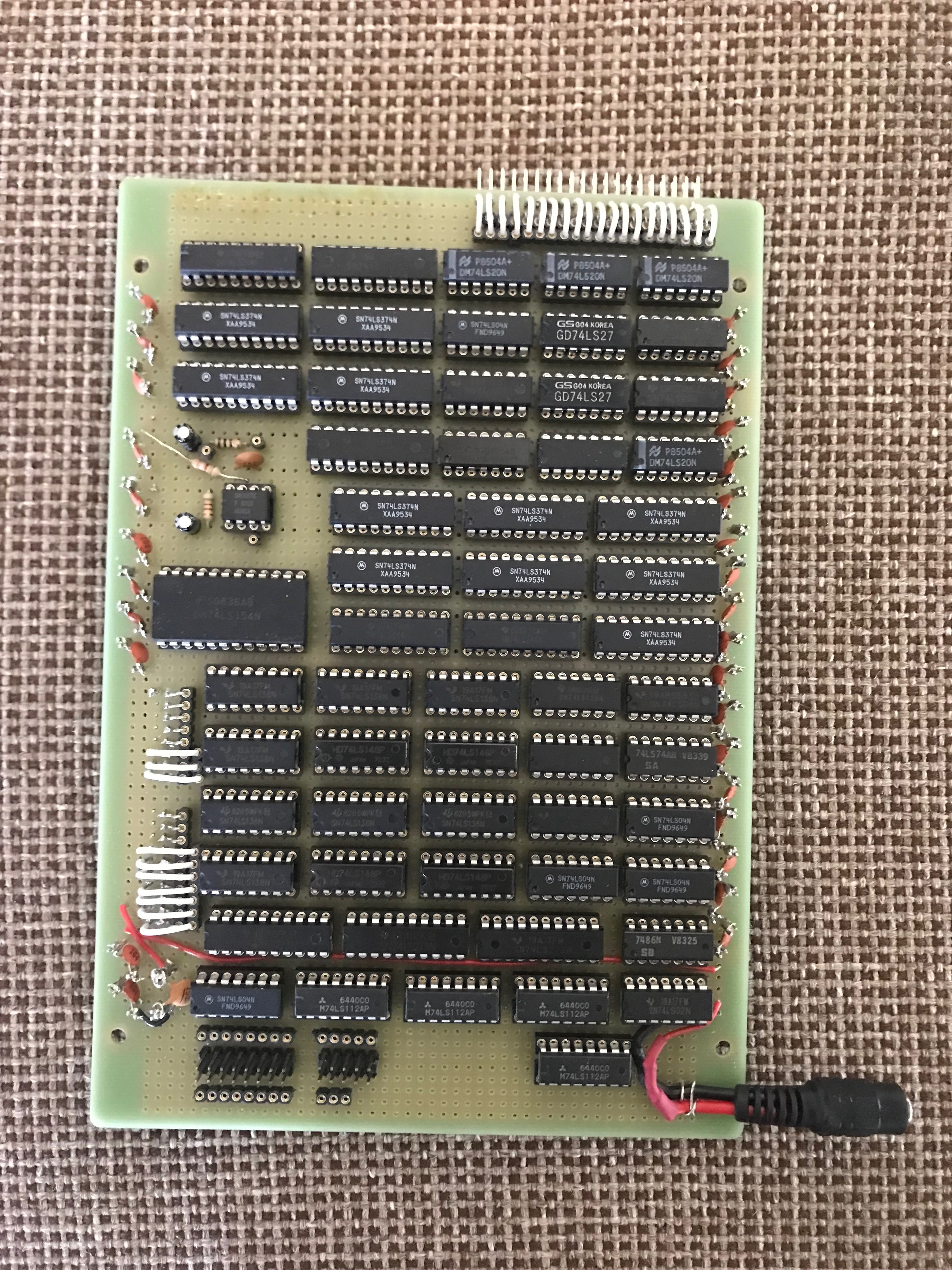
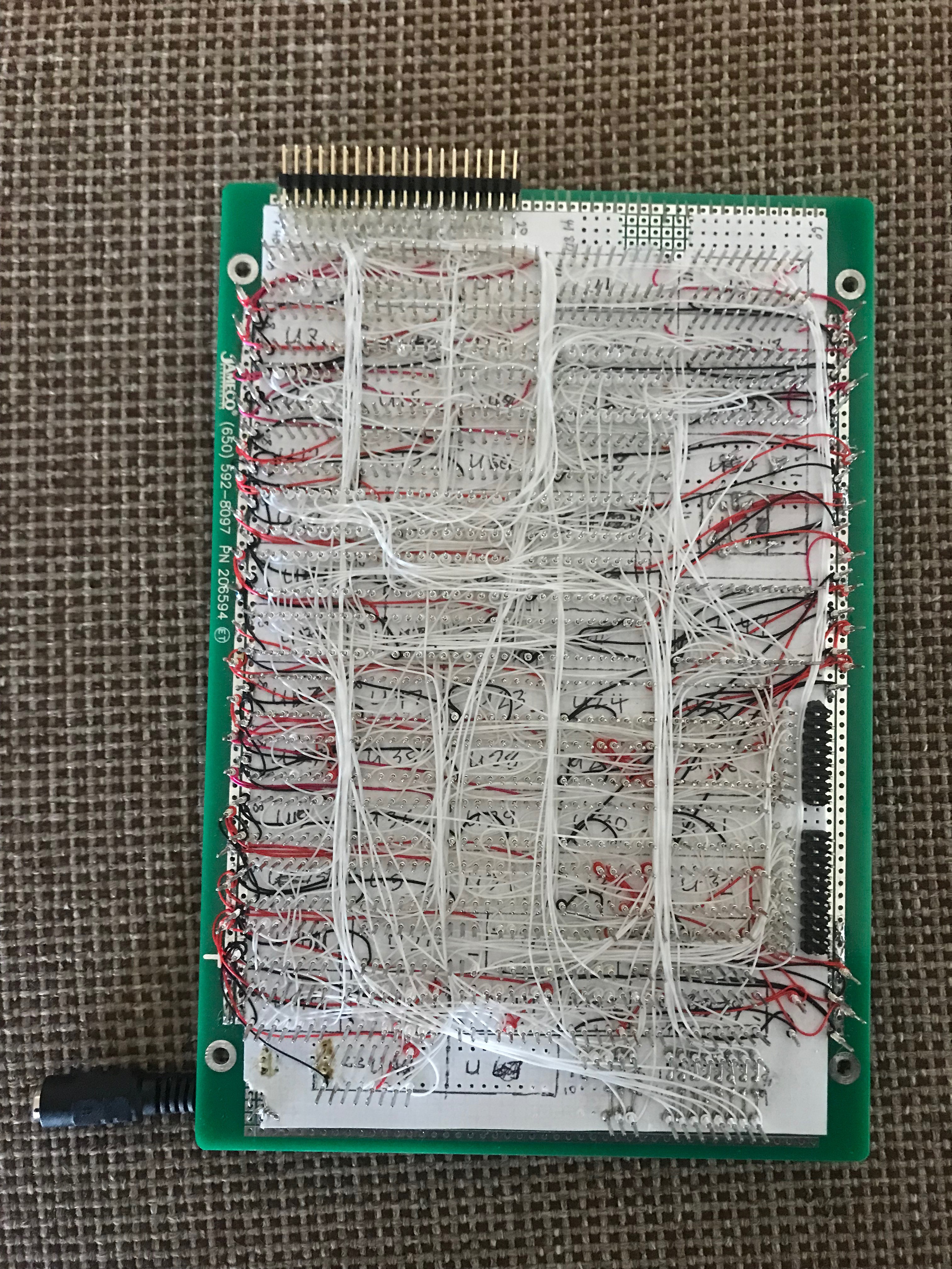
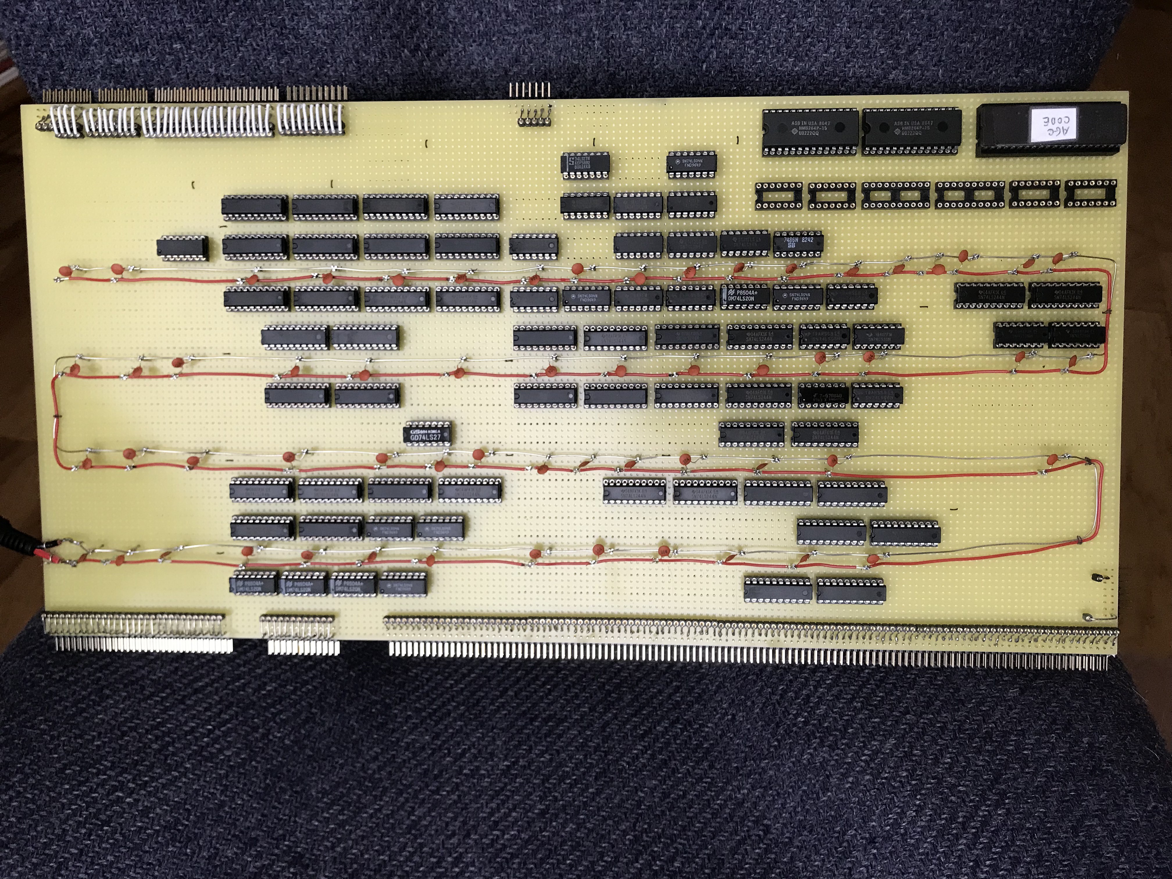
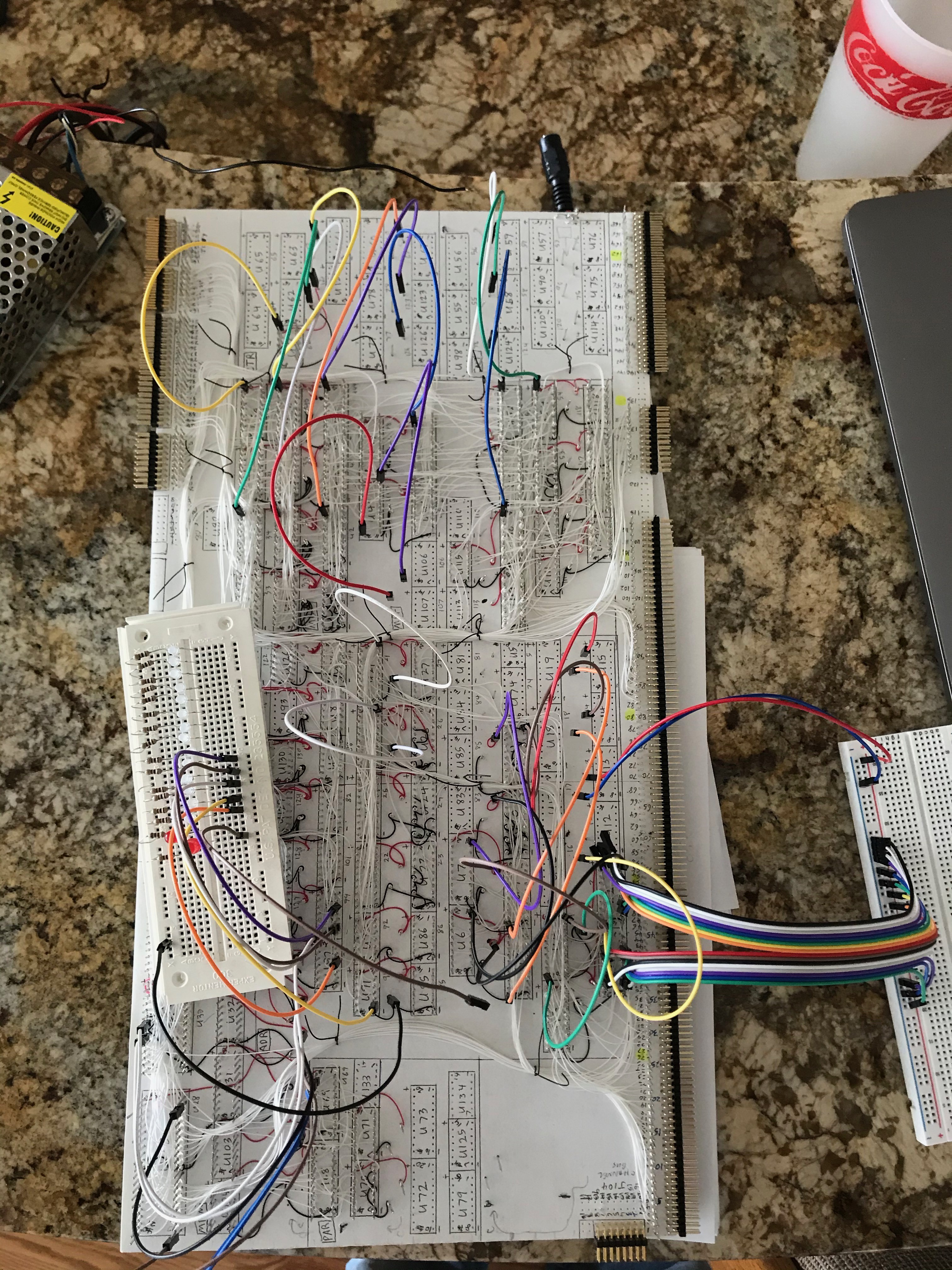
    This is where I started.  I added the code EPROM and RAM, then started adding various access registers before I became overwhelmed using just my simple 16-bit register viewed.  I realized I needed the Display sub-system so I switched gears and have been working on that.  Here are some pictures of where I am to date.

    Even though I have the AGC Code EPROM plugged in, I will probably start with some simpler test programs I have created to test various commands that never seemed to come up in the AGC code.  Some of that code contains the more complicated multiply and divide instructions.  The documentation has good test case scenarios that I used to make sure they are working.

    Here are some design notes that help understand the schematics.

    Erasable/Fixed Memory: This module contains a single EPROM chip that contain the code which was generated using the modified assembler. This is a 16-bit data by 16-bit address chip that can handle all the code in the Luminary 099 program. There are also two RAM chips that implement the erasable memory.

    The single 16-bit EPROM brings some simplification from a chip count, however it is more complicated from an implementation standpoint. The data lines are a bit reversed from what you might expect. The bytes are reversed and I did not attempt to change this as it is easier to read and verify in this configuration. From a hardware perspective, it is a simple matter to switch the byte's data lines. If the address is 0 then the first data word is 1687 hex. Given this, the data lines are as follows.

    1 = D7 – D4
    6 = D3 – D0
    8 = D15 – D12
    7 = D11 – D8

    The address lines are as you would expect when dealing with the EPROM. For instance, address 4000 octal equals 800 hex which will give a data value of 0004 hex. The S-Record format is what is a bit strange. The data is defined a byte at a time. To see this data value in the S-Record file, double the address value. In the case of 4000, double 800 hex gives a value of 1000 hex. Looking at the S-Record values at this location you will see 00 04 38 2c.

    Memory Buffer: This module encapsulates the G register. All data in and out of memory go through this register. The shifting when writing to addresses 20, 21, 22 and 23 occur in this module. Data arrives via the Write Bus and Direct Write Bus. The data read from fixed memory is checked for specific values; all zeros or GMZ, EQ3, EQ4 and EQ6. The EQ pulses check for the TC instructions that translate into the RELINT, INHINT and EXTEND instructions.

    The determination of the four specific G register values results are straight forward except the combination of the CYR and SR. All the bits are the same except bits 14, 15 & 16. The table below shows the values.

    BitW20W21Equation
    14B15B16(!W21 * B16) + (!W20 * B15)
    1510W21
    160B16(!W21 * B16)

    Parity: This module in Block I was driven by control pulses within the Control Pulse Matrix. In Block II they realized you always generate parity when writing to memory and test parity when reading from memory. I kept the control pulses as internal pulses to drive this functionality. I chose to implement parity for the erasable ROM memory, but not for the fixed memory. It would be easy enough to implement this if you wanted to.

    This functionality is implemented using two parity generator chips. This module contains the P register and PALM (parity alarm) single bit register.

    Interrupts: This module implements three of the interrupts; the keyboard interrupt along with TIME3 and TIME4. The inhibit interrupts is also implemented in this module. A RPCell register maintains which interrupt has occurred. When an interrupt is processed, this module converts the specific interrupt into the memory address of the code's interrupt jump table. The address equals 04000 + RUPT # << 2. The addresses are (in octal).

    4014 = RUPT3(TIME3)
    4020 = RUPT4 (TIME4)
    4024 = RUPT5 (KBD

    Counters: This module implements four of the counters. The...

    Read more »

  • Display

    wglasford07/06/2022 at 23:47 0 comments

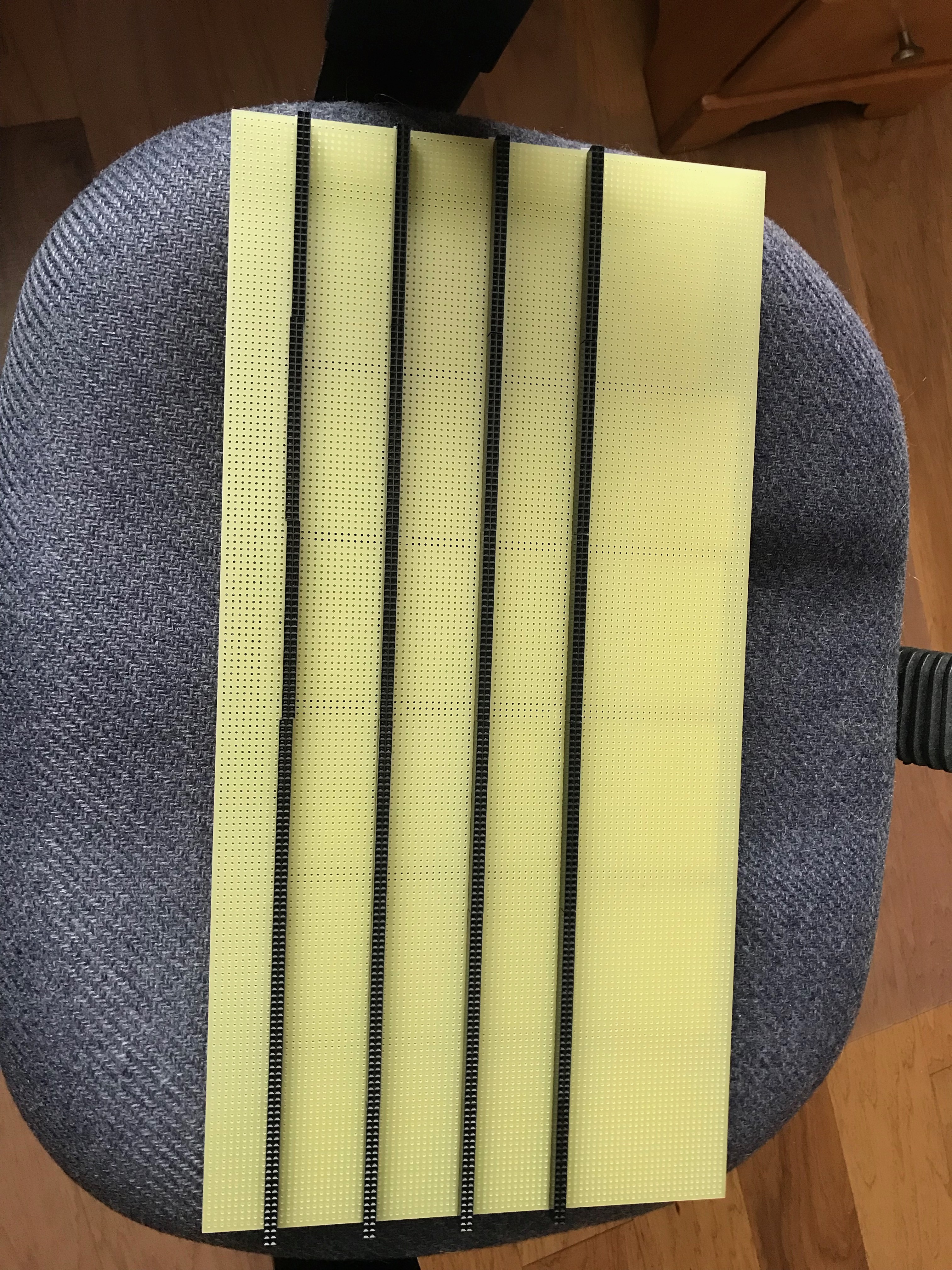
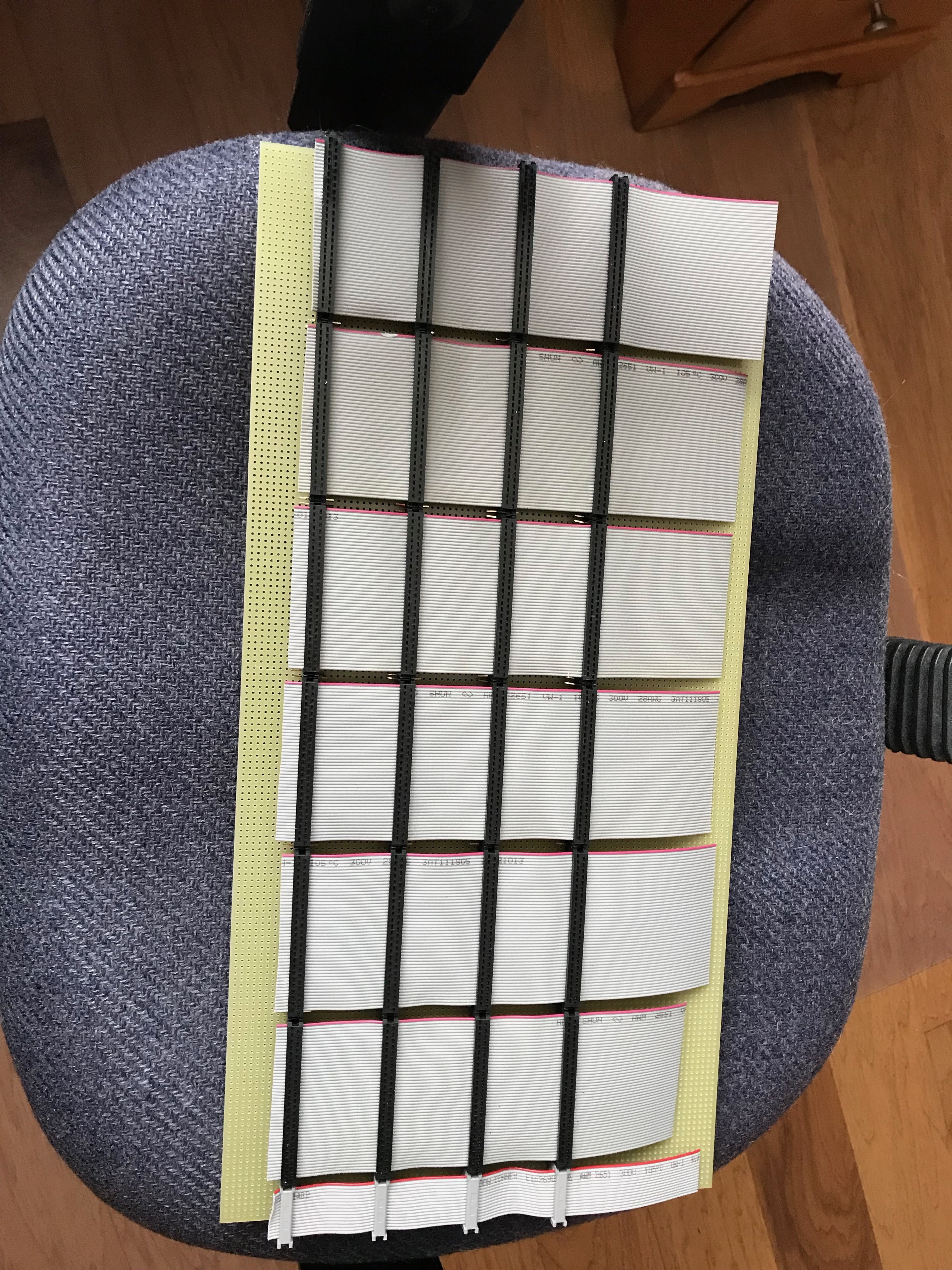
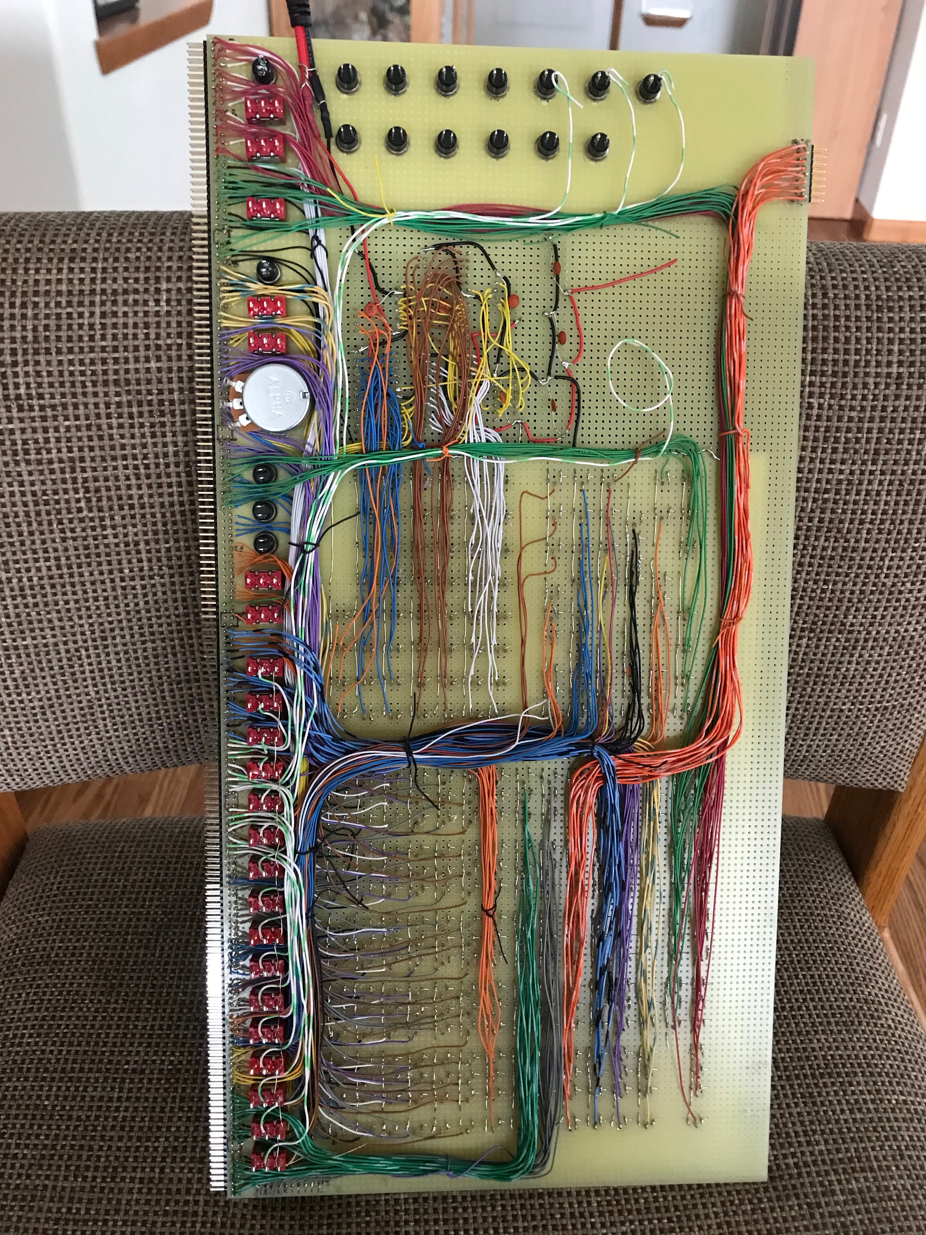
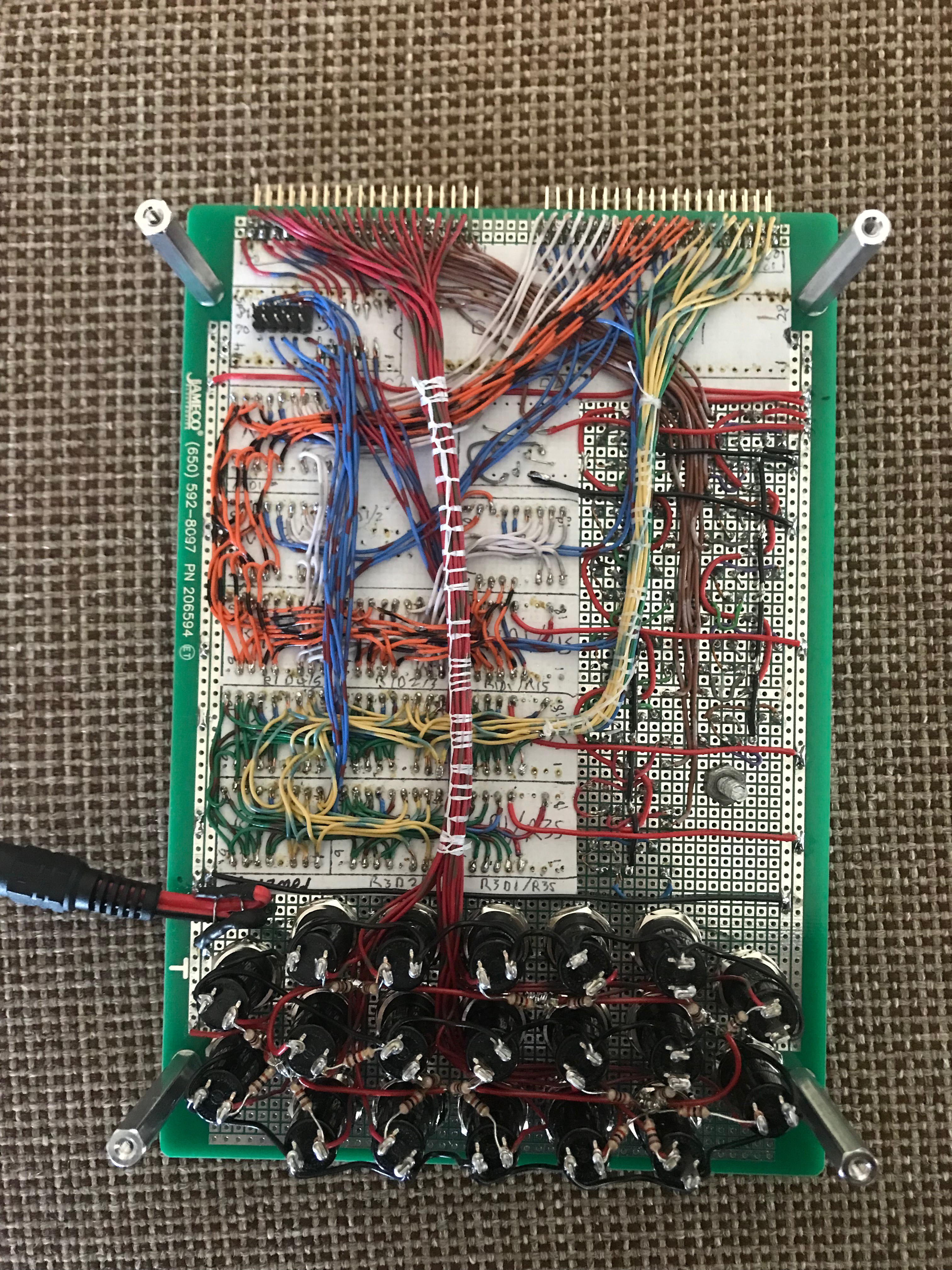
    I started wiring up the Memory sub-system board and realized quickly that I needed the display board to show the state of the various registers.  I first had to create a backplane to connect the boards into.  The backplane carries all the signals the display board requires.  The display functionality was not part of the original AGC.  This functionality is based on my simulator and what I needed to control the simulation.  The actual computer required data and control signals are routed via ribbon cables on top of the boards.

    Here is the backplane.  Notice that I left room for an additional board, just in case.  I had to make all the  connector cables and slots universal so I could move the board under test to the back of the stack to have access  to the wire wrap pins for debugging purposes.

    The display panel has LEDs grouped by register.  In the middle of the board is an array of sub-sequences showing which sub-sequence is being executed.  All of the controls that are available on the simulator are available here, including a row of 16 data/address input switches.  I chose to solder this board and the front board of the DSKY.  All remaining boards are wire wrap for easy modification when I make that inevitable mistake.

    All the LEDs are wired up and tested.  I am working on the switch logic.  

    Here are some of design notes that help understand the schematics.

    The backplane is used to route all LED and switch lines between the logic boards and the display board. There are 338 connectors (169 * 2). If a NOT gate is required for the LED to show positive logic, then that is placed on the logic board.

    The lines are laid out so that each of the three logic boards (CTL, MEM, PROC) do not have doubled up or overlapping pins. This way only one row of wire wrap terminals are required. It also strengthens the connection as more pins are anchoring the boards. The schematics use global labels to identify connections to the backplane due to the limitations of drawing real estate. The backplane connectors are shown on the interface drawings as single row connectors. The largest connector is 40 pins so multiple 40 pin connectors are required. The global labels on the hardware diagrams are numbered as per the list below.

    The pin layouts identify two rows; A & B. The purpose column identifies the subsystem-module purpose with the number of connections in parenthesis. Note: The register and memory switch LSBs are the lower number, the higher number is the MSB. There are two unused pins every 25 pins due to the space required for the backplane ribbon cable connectors. The following tables shows the pin assignments.

    Row A:

    Pin #Purpose
    1-16MEM-EFM: Memory Bus (1-16)
    17-25MEM-ADR: S Monitor Bus (1-9)
    26-27Unusable
    28-30MEM-ADR: S Monitor Bus (10-12)
    31-39MEM-ADR: Bank Monitor (9)
    40-52MEM-ADR: Address Bus (1-13)
    53-54Unusable
    55-57MEM-ADR: Address Bus (14-16)
    58MEM-MBF: EQU3
    59MEM-MBF: EQU4
    60MEM-MBF: EQU6
    61MEM-ADR: EQU17
    62MEM-ADR: GTR7
    63MEM-ADR: GTR1777
    64MEM-MBF: GMZ
    65MEM-CTR: INC TIME1 (1)
    66MEM-CTR: INC TIME2 (1)
    67MEM-CTR: INC TIME3 (1)
    68MEM-CTR: INC TIME4 (1)
    69MEM-ADR: Examine Memory Pushbutton (1)
    70MEM-ADR: Examine Next Pushbutton (1)
    71MEM-EFM: Read/Write Switch (1)
    72MEM-ADR: AGC/Manual Switch (1)
    73MEM-ADR: Clear Parity Pushbutton (1)
    74MEM-EFM: Load Memory Pushbutton (1)
    75MEM-INT: RUPT3 Switch (1)
    76MEM-INT: RUPT4 Switch (1)
    77MEM-INT: RUPT5 Switch (1)
    78MEM-PAR: PR_1-15 (1)
    79CTL-MON: SA (1)
    80-81Unusable
    82-97MEM-MBF: G Monitor Bus (1-16)
    98-106MEM-ADR: Memory Switches (1-9)
    107-108Unusable
    109-115MEM-ADR: Memory Switches (10-16)
    116CTL-MON: BPEN (1)
    117CTL-CLK: Clock Control: 1 MHz / Slow (1)
    118CTL-TPG: IBPEN (1)
    119CTL-CLK: CLK1 (1)
    120CTL-TPG: CBPEN (1)
    121CTL-MON: RUN – Exec. Mode (Run/Step) (1)
    122CTL-MON: INST – Exec. Control (Instruction/Sequence) (1)
    123CTL-MON: FLCK – Clock Mode (Run/Step) (1)
    124CTL-MON: Master Reset Switch (1)
    125CTL-MON: STEP – Exec. Step (1)
    126CTL-MON: MCLK...
    Read more »

  • DSKY

    wglasford07/06/2022 at 23:31 0 comments

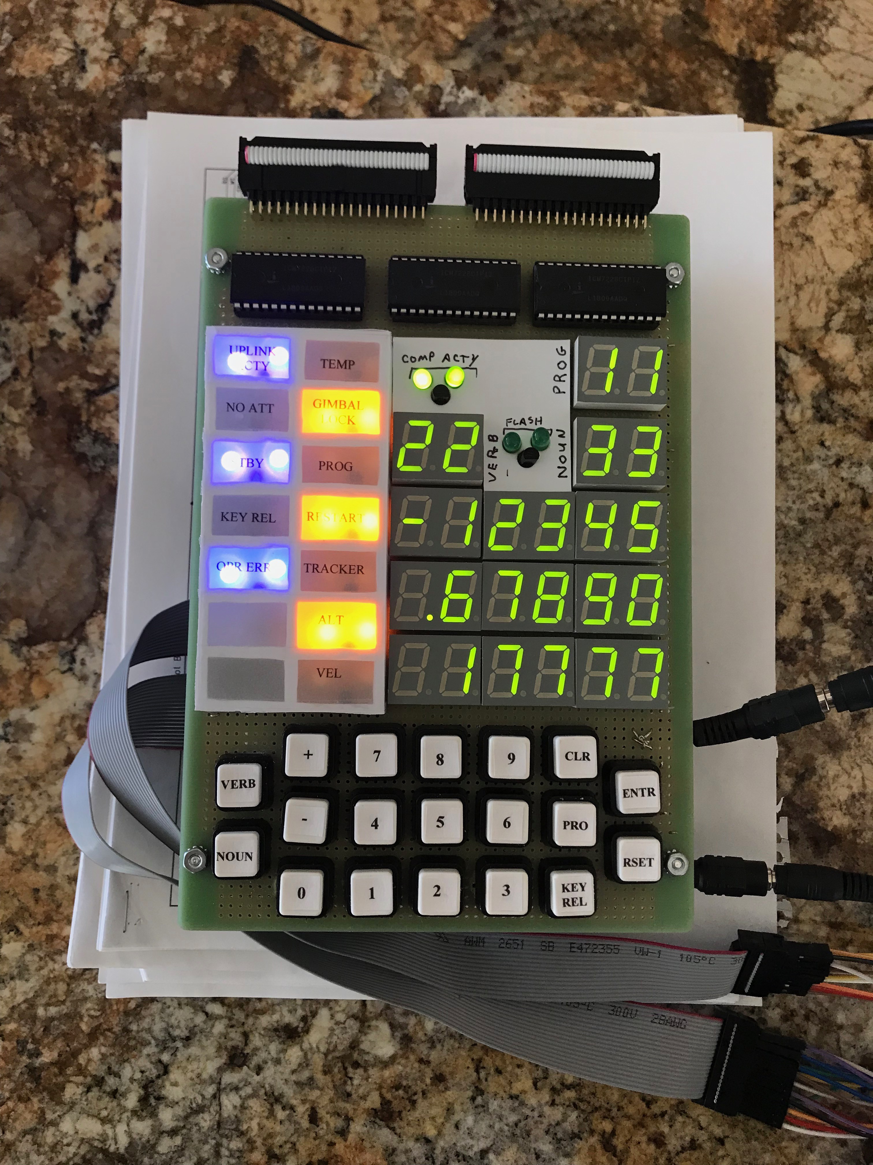
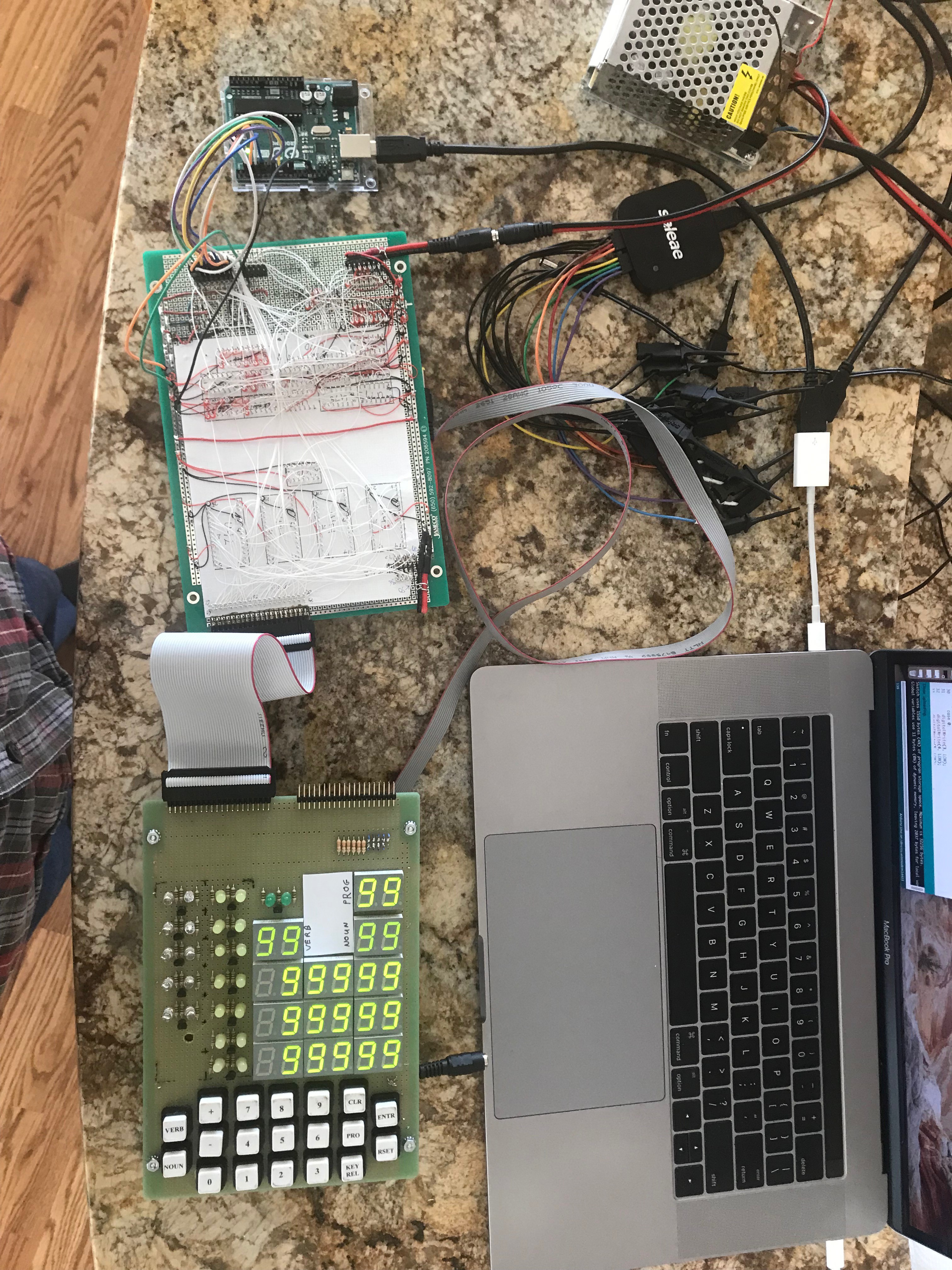
    The DSKY is a separate physical piece of hardware with a simple interface consisting of the 15-bit channel bus and a handful of control signals.  I built this as a stand-alone piece that started out as two boards and then grew to three boards.  I have tried two different implementations and have finally settled on a third implementation.  This has been slow going as during the pandemic I have been stymied with a shortage of certain chips.  I first tried using only simple TTL chips and it got a bit too complex.  I then discovered an LED driver chip and decided to go with those.  I purchased three of these chips and discovered I needed a fourth and I have been waiting for 6 months for availability to complete this sub-system.

    I test this sub-system with a Raspberry Pi driving the data lines.  Here is picture of that setup.

    As soon as I get the remaining chips I need I will complete this sub-system.  In the mean time I made a paper model of the DSKY and that sent me down the path of building a better looking model of the DSKY.  See my DSKY Model project for the progress on that DSKY.  Both DSKYs are designed to connect to the AGC.

    Here are some of the design notes that will help understand the schematics.  

    Keyboard: This module implements 19 switches. These switches are converted into a keyboard code using gate logic that is stored in the Channel 15 register. The keyboard codes, their meaning are defined in the following table.

    KeyABCDEID
    1000011
    2000102
    3000113
    4001004
    5001015
    6001106
    7001117
    8010008
    9010019
    0100000
    Verb10001a
    Reset10010b
    Key Rel11001c
    "+"11010d
    "-"11011e
    Enter11100f
    Clear11110g
    Noun11111h

    The keys are pushbuttons that are normally high. A keypress presents a zero to the logic equations. Negative logic presents the easiest solution. All the lines of interest are normally 1. The logic for each of the five code bits is looking for a key to go low. The logic equations utilize 3 and 4 input NAND gates along with 2 and 3 input NOR gates. The results is NOTed. The equations are as follows.

    A = (a * b * c * d) + (e * 0) + (f * g * h)
    B = (8 * 9 * c * d) + e + (f * g * h)
    C = (4 * 5 * 6 * 7) + (f * g * h)
    D = (2 * 3 * 6 * 7) + (b * d * e * g) + h
    E = (1 * 3 * 5 * 7) + (9 * a * c * e) + h

    Notice that some of the portions of the equations are the same. For instance, A, B and C both have the (f * g * h) portion.

    Display: The Display module implements the Channel 10 and 11 registers. Channel 10 is used to write data to the 7-segment LEDs two LEDs at a time. Channel 11 is used to light various indicators. Eight indicator are controlled using Channel 11. Another eight are controlled using Channel 10 with a specific relay word.

    It should be noted that all the miscellaneous timing pulses using 555 chips are set up as astable multi-vibrators.

    Most of the display logic decodes the Channel 10 value which is used to drive the 7-segment displays as pairs of numbers. Each output to this register drives two 7-segment numbers along with the plus/minus signs and a few other indicators. The format of the register is bits 1-5 hold a low digit value (DSPL), bits 6-10 hold a high digit value (DSPH), bit 11 indicates the plus/minus sign (DSPC) and bits 12-15 contain the relay word (RLYWD).

    RRRRSHHHHHLLLLL

    According to Ron's website, it is unclear how to blank the sign LEDs. There is one that says light the “+” sign and one that says light the “-” sign. Ron chose to display a blank if both values are zero. There is also the case where both may be set. I am not sure if this is avoided in code, but I have decided to handle this as a blank the sign case. The following table shows the possible states and the results.

    (+) State(-) StatePlusMinus
    0000
    0101
    1010
    1100

    The relay words and the digits each one drives is listed below.

    RLYWD#DSPCDSPHDSPL
    101111n/aMD1MD2
    101010FlashVD1VD2
    10019n/aND1ND2
    10008UPACTn/aR1D1
    01117+R1SR1D2R1D3
    01106-R1SR1D4R1D5
    01015+R2SR2D1...
    Read more »

  • Hardware Drawings

    wglasford07/06/2022 at 23:15 0 comments

    Up to this point I have been in my comfort zone, having spent my career as a software developer.  Now it is off into the unknown of hardware development.  The first thing I need is a good schematic drawing tool.  After some research I decided to use KiCad.  It is free, easy to use and seems to be what all the cool kids are using.  

    Note that all my schematics are out on my GitHub site at https://github.com/bglasford1 under the AGC Block II Computer project in the schematics directory.  I chose to divide the project into five sub-systems; DSKY, Control, Processor, Memory and Display.  The DSKY sub-system consists of the Keyboard, Display and Indicator modules.  The Control sub-system contains the Clock, Scalar, Timing Pulse Generator, Sequence, and Control Pulse Matrix modules. The Processing sub-system contains the Arithmetic Logic Unit and Central Register modules. The Memory sub-system contains the Erasable Fixed Memory, Memory Buffer, Parity, Memory Address, Interrupts and Counters modules. The Display sub-system contains the Monitor module along with all the LEDs and switches from the Control, Processing and Memory sub-systems.  The basis for splitting the modules up into sub-systems was to group like modules and to evenly divide them onto individual boards based on initial chip count.  

    I first had to create some data flow diagrams to visualize how this beast would be wired together and what pieces relate to other pieces.  The data flow diagrams depict how the buses and registers interact with the control signals. The registers and logic blocks are rectangles and the bus drivers are round-tangles. The control signals that drive data into/out of registers and bus drivers are shown. The bus drivers and registers that are activated by the CLK1 pulse are colored green, the ones activated by the CLK2 pulse are colored yellow and the ones activated by the CLK3 pulse are colored cyan. This allows a quick visualization of the multi-stage data flow control during a single timing pulse.

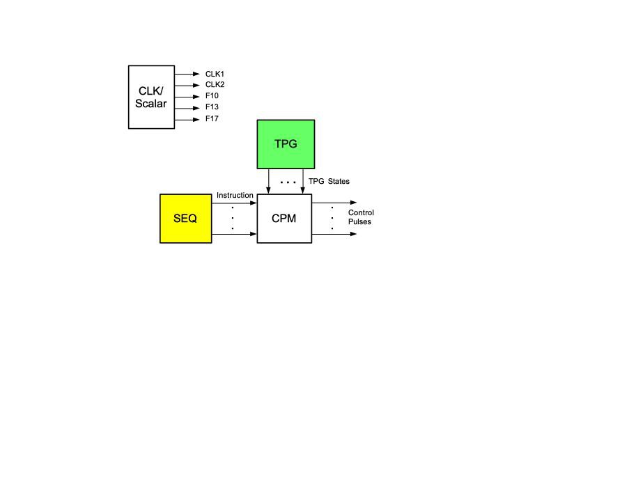
    The following data flow diagram shows the overview of the control sub-system which includes the Timing Pulse Generation, Sub-sequence and Control Pulse Matrix modules as well as the Clock and Scalar modules. The Clock and Scalar modules simply create various clock pulses. The Timing Pulse Generation module uses a slightly delayed CLK1 pulse to transition between 12 timing pulse states as well as a few other debug states. The Sub-sequence module maintains the parts that make up the next instruction, to include the stage, sequence and branch values. These along with the timing pulse state are fed into the Control Pulse Matrix module which uses these values to look up the control signals from the control pulse matrix EPROMs. These control signals along with other internally generated signals cause the other modules to perform actions. These control pulses are generated during the rising edge of the CLK1 pulse. The other modules act on the read control signals immediately and delay the write signals until the start of the CLK2 pulse.

    The Timing Pulse Generator is a state machine that controls the states a sub-sequence goes through. This includes the start up states and states that allow one to debug the system. Many of the states loop back on themselves, waiting for a specific input to transition them to the next state. Once in the TP1 state, the state machine transitions through to TP12 each clock pulse. The intermediate states are not shown for clarity. At TP12 the state can transition to a wait state if a breakpoint is set or to standby if the standby switch is set or loop back to TP1 if free running. Notice that if none of these states is set it simply transitions to the wait state. The wait state is preceded by the Switch Release state. Under each state name is a number that is the internal numeric depiction of the state.

    The following data flow diagram shows the memory...

    Read more »

  • Simulator

    wglasford07/06/2022 at 22:44 0 comments

    What sent me down this path was when I was looking for an historically significantly computer to build. I found John Plutorak's implementation of the AGC Block I computer.  This was what I was looking for.  I decided to push the boundary by focusing on the Block II version as that is the version that landed men on the moon.  John built a hardware based simulator, but he wrote it in C and I much prefer Java.  

    I built a simulator that runs Block II code and provides a nice GUI interface to execute the simulation.  The input files consist of the following S-Record files; the CPM files, the machine code file and a sub-sequence file.  

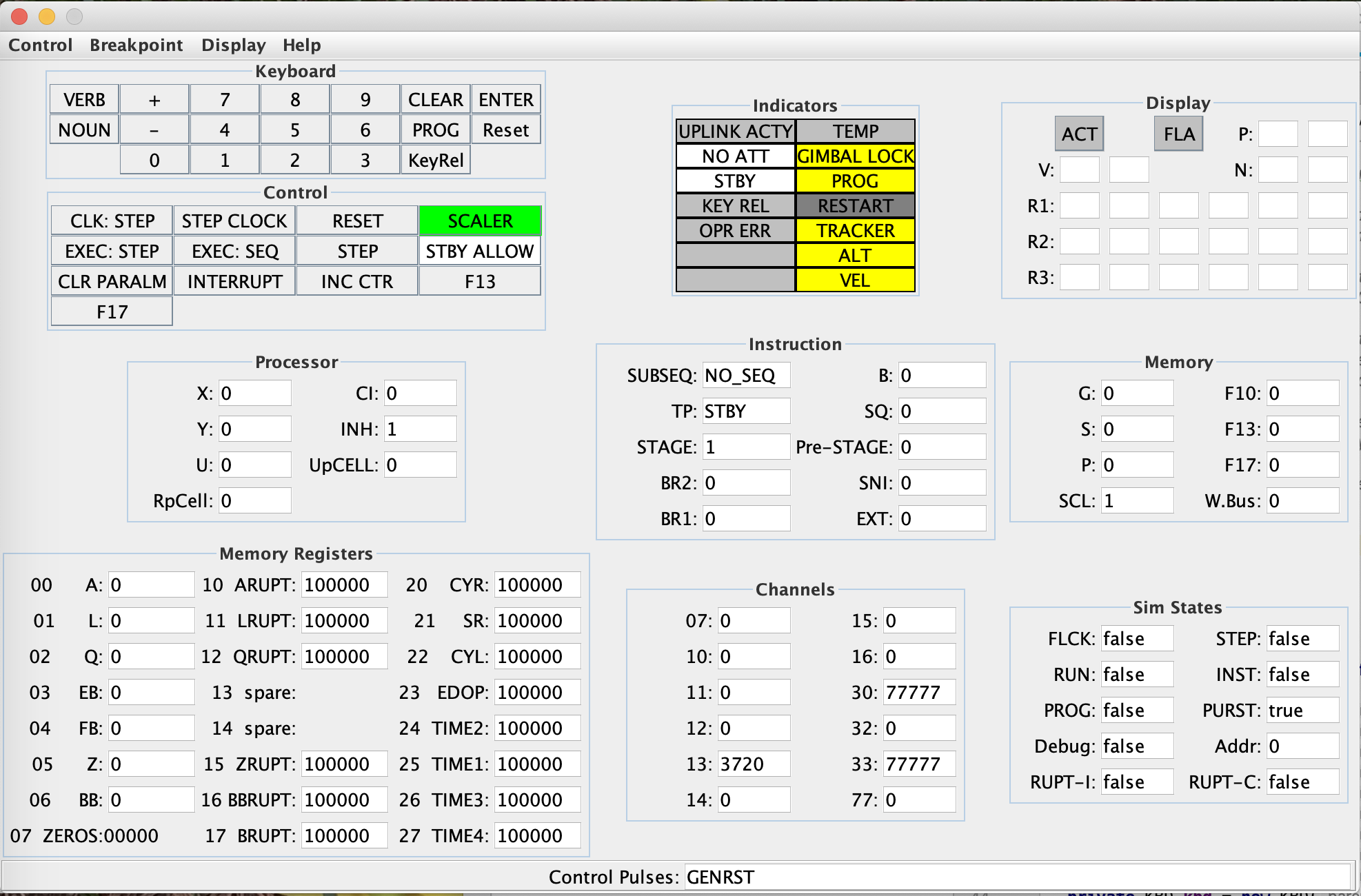
    Here is a screen capture of the simulator GUI.  Notice that there are sections that simulates the DSKY, namely the Keyboard, Indicators and Display.  The Control section is used to control the simulator.  The help menu has an explanation of how to control the simulation.  You can step through individual instructions, through each sub-sequence or even step through the timing pulses.  After I got a few instructions working I realized I needed to set a breakpoint and let the simulator free run to that point.  You can also break on a specific interrupt or counter increment.  There are Sim States that give you insight into the state of the running simulation.  The remainder of the sections are the actual registers and key memory locations within the computer.  As instructions are executed you can see how each register is affected. This screen is going to translate into a whole lot of LEDs.

    As before, all the source code and files required are out on my GitHub site.

  • Assembler

    wglasford07/06/2022 at 22:30 0 comments

    Ron provided an assembler and all the available assembly listings.  People went to museums and hand entered the assembly code and verified it by assembling the code and running it through Ron's simulator.  That was a HUGE effort and HUGE thanks to everyone involved in that effort.  

    All I did was extend the assembler by adding an option to output the machine code in a Motorola S-record format.  I use this output file as an input into my version of the simulator and as input into my ROM burner to burn the code into an EPROM for the hardware I am developing.

    My modifications to Ron's assembler can be found on my GitHub site at https://github.com/bglasford1 Under the AGCBlockIIComputer project there is a YUL directory that contains my modifications.  The original assembler was named YUL because they had a Christmas deadline.  You can recreate the assembler I am using by first downloading Ron's yaYUL code and then adding my modifications to it.

  • Understanding how the computer works

    wglasford07/06/2022 at 22:19 0 comments

    Fortunately most of the NASA documents are available.  They can be found on-line at  https://www.ibiblio.org/apollo/Documents/ 

    The following documents are what I leaned heavily on in gaining an understanding of how this computer works.  

    R-393.pdf → Logical Description for the Apollo Guidance Computer (AGC4)

    E-2052.pdf → AGC4 Basic Training Manual

    1689.pdf → AGC4 Memo #9 – Block II Instructions

    R-700.pdf → Computer Subsystem

    AGC Information Series, ISSUE 32 Block II Machine Instructions

    That last document is the most important.  Without it I would have been guessing.  That document shows each instruction and the control pulses required to execute the instruction.  The control pulses are stored in a Control Pulse Matrix.  There are a few slight errors in the CPM laid out in this document, but I found the correct version in other documents.  The original CPM was created using a matrix of diodes.  I chose a simpler, more modern method, burn the information into an EPROM.   

    In the original R-393 document, Chapter 2 describes blocks of functionality diagramed in Figure 2-1. I have choose to refer to these blocks as modules. There are 17 modules described below; 15 from the original documentation and an additional module used to monitor and debug the hardware plus I added a pseudo module to describe the Channels. In the implementation, there is no Channel module as this functionality is parsed out into other modules. The modules are as follows:

    1. Clock
    2. Scalar
    3. Central Registers
    4. Arithmetic Logic Unit
    5. Sequence Generator
    6. Timing Pulse Generator
    7. Control Pulse Matrix
    8. Interrupts
    9. Counters
    10. Memory Address
    11. Memory Buffer
    12. Erasable/Fixed Memory
    13. Parity Generator
    14. Keyboard
    15. Display
    16. Channels
    17. Monitor

    Data Format: A computer word is 16 bits in length. The math is primarily 1's compliment arithmetic. The instruction word consists of a 3 bit opcode, 12 bit operand and 1 parity bit. The single parity bit exists to detect single bit memory errors. The data word is similar in that it consists of 14 bits of data, and two sign bits.

    When data is moved from memory into a central register, the parity is automatically checked and then the parity bit is replaced by a sign bit, so a central register word consists of the same 14 bits of data and two sign bits. The sign bits decode as follows.

    Bit16Bit15Meaning
    00Positive
    11Negative
    01+ Overflow
    10- Overflow

    Block II introduced the concept of double precision numbers. This is why the L register was moved next to the A register so the two registers together can make up a double precision number. With A being the more significant number and L being the lower. The format for a double precision fraction is +/- A * +/- 2 ** B where the sign of A is the overall sign of the number and the sign of B is the sign of the exponent.

    Buses: In Block I there was a read bus and a write bus. This was a strange concept that did not survive in Block II. The newer documentation refers to the single data bus as the write bus. There are also added buses that move data directly from the A to X register and between the L and G registers. These two buses facilitate some of the time reduction of the multiply and divide commands. The Channel Bus was added in Block II to free up erasable memory.

    The Clock (CLK) module is simply a 4 MHz crystal that provides the heartbeat of the system. This module divides the 4 mHz pulse by four to produce four non-overlapping 1 MHz clock signals. The clock signals are used to trigger various internal operations. The reason for more than one clock signal is that if you simultaneously assert the RA and WB control pulses to move data from the A to B registers you will not get consistent results. The data must be on the write bus before the WB pulse latches the data. Both control pulses are asserted simultaneously, however you must first assert the RA control pulse to place the data onto the write bus, then a short time later assert...

    Read more »

View all 10 project logs

Enjoy this project?

Share

Discussions

zpekic wrote 09/18/2022 at 14:48 point

Fascinating and ambitious project, wishing you best of luck! I need to dig in more, but one question jumped out right away: what is the plan / approach to test the CPU? After all, the original only executed the actual moon landing mission code, which is probably available, but without right sensor inputs (or mocking their values in some way) its execution would not go far. Do you plan some test code, similar to what other CPUs have (I ran some on my Am9080 "implementation" in FPGA and it failed miserably, although monitor program ran without much problems, so I know that making a replica in any technology is hard). 

  Are you sure? yes | no

Similar Projects

Does this project spark your interest?

Become a member to follow this project and never miss any updates