 Peter
PeterOverview
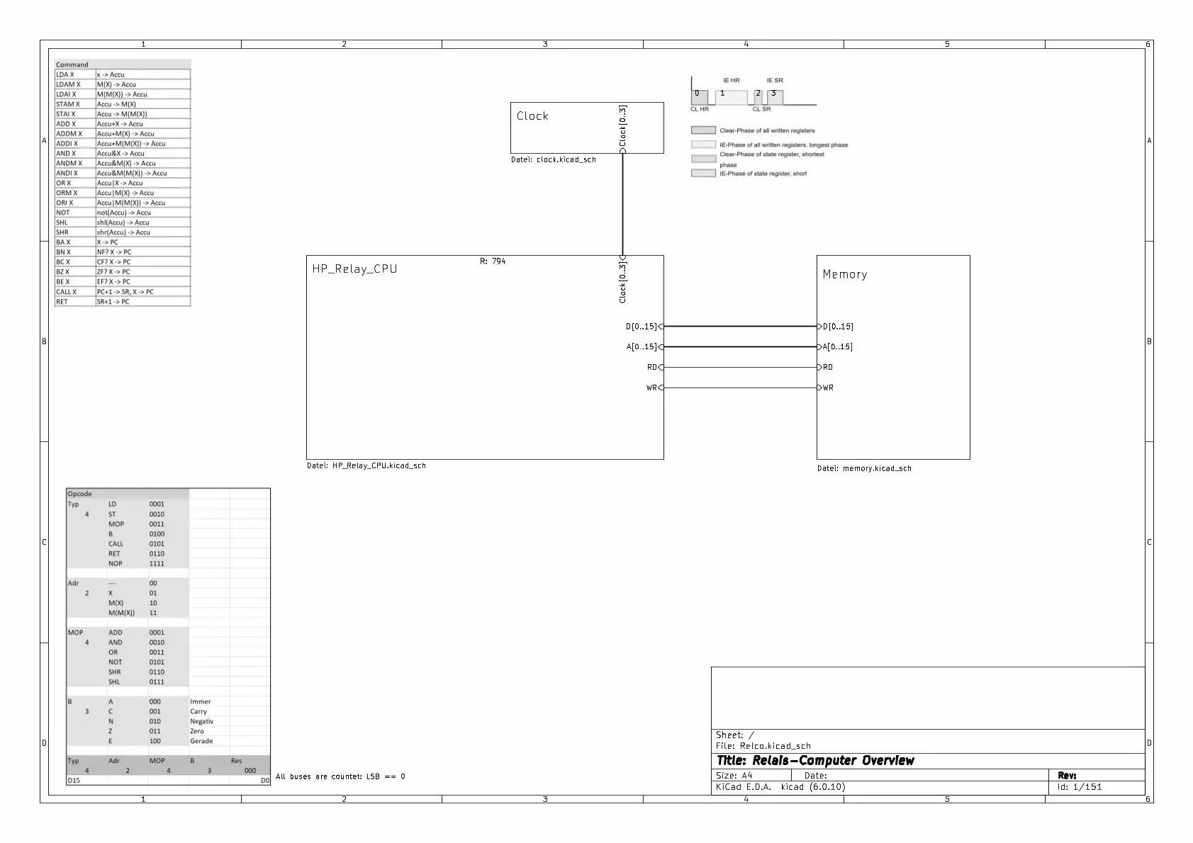
The system ist a very simple CPU using an Accu register like CPUs in the 80s. The following table shows the command set of the CPU, the picture below the register structure.
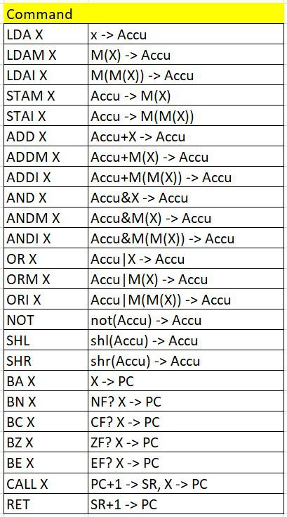
The CPU is able to adress the memory using 3 different adressing modes. a) LD X is loading the Accu with the dataword stored in the adress after the opcode, b) LD M(X) is loading the Accu with the data stored in the memory adress stored after the opcode, and c) LD M(M(X)) is ... yes, indirect adressing. The dataword after the opcode contains the adress where the CPU finds the adress of the dataword that will be stored in the Accu. Is adressing mode c) really necessary? Maybe not. But it makes it easier.
And, as you can see, a CALL / RET set of operations is also avaliable. No, there is no stack realized, only one subroutine level is possible. The return adress is stored in the register SR.
The CPU is a classical Accu machine. All mathematical operations are using the Accu, also all store / load operations. And, because it is a "High Performance" relay system, the program counter has its own adder which is only able to add 1 to the program counter.´
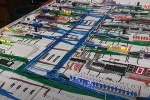
The Simulation using "Logic World"
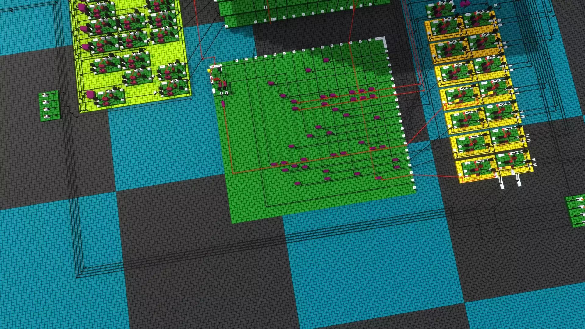
The following images show the Simulation of the complete system:
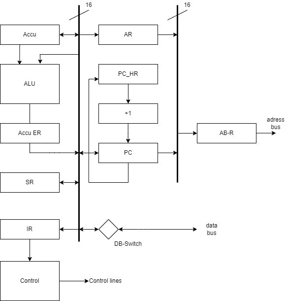
The relay element:
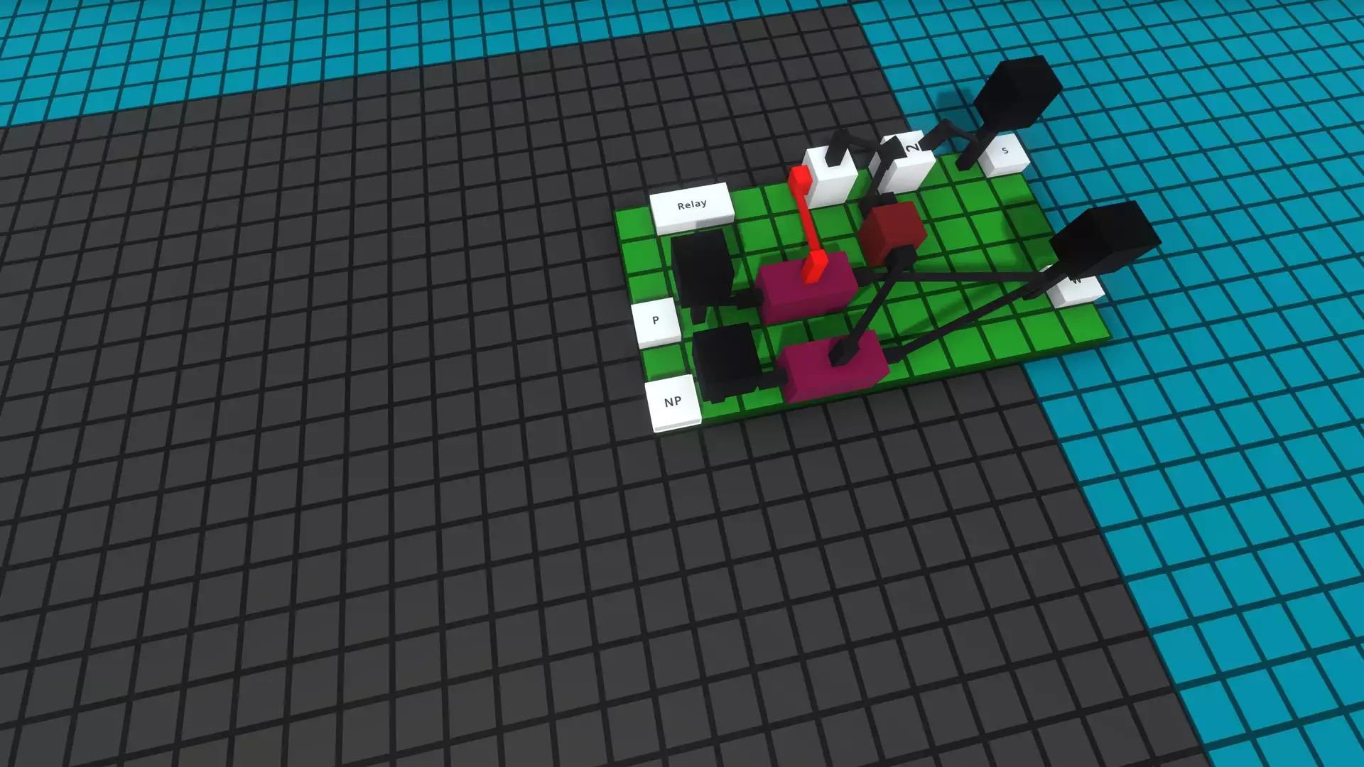
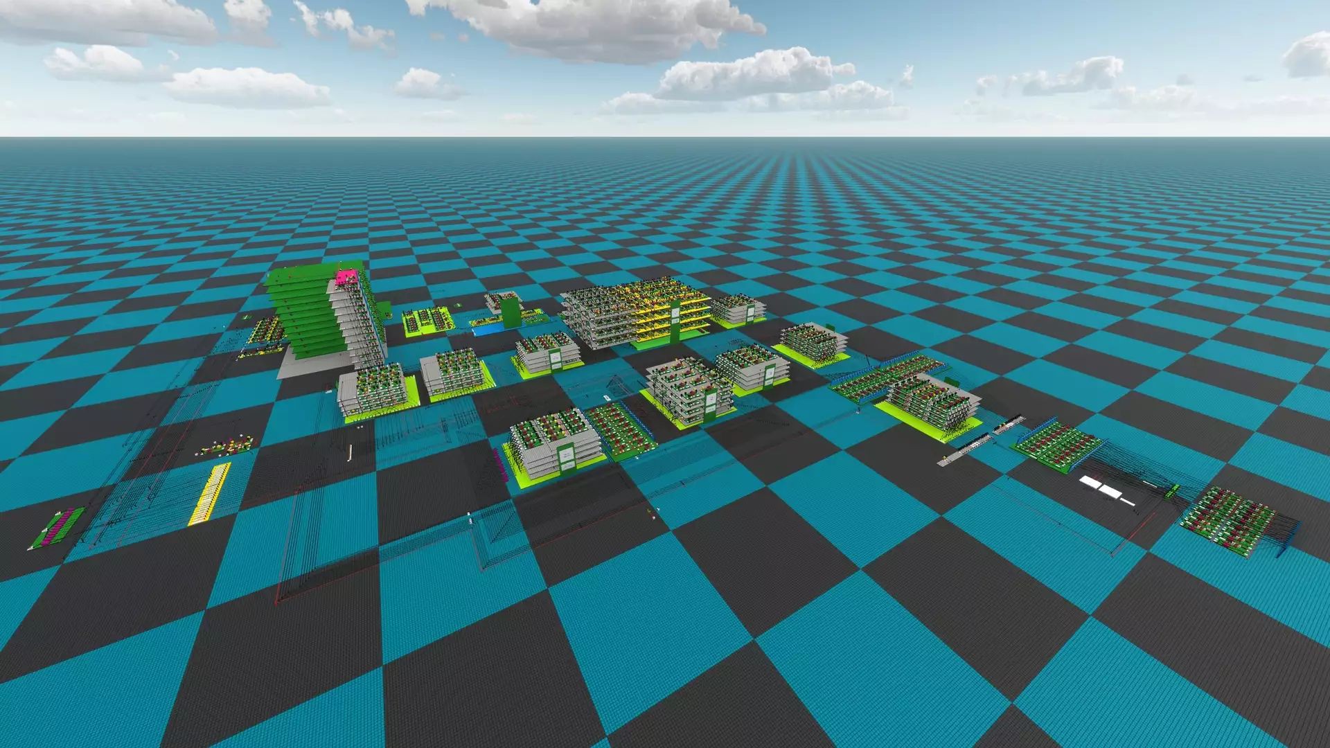
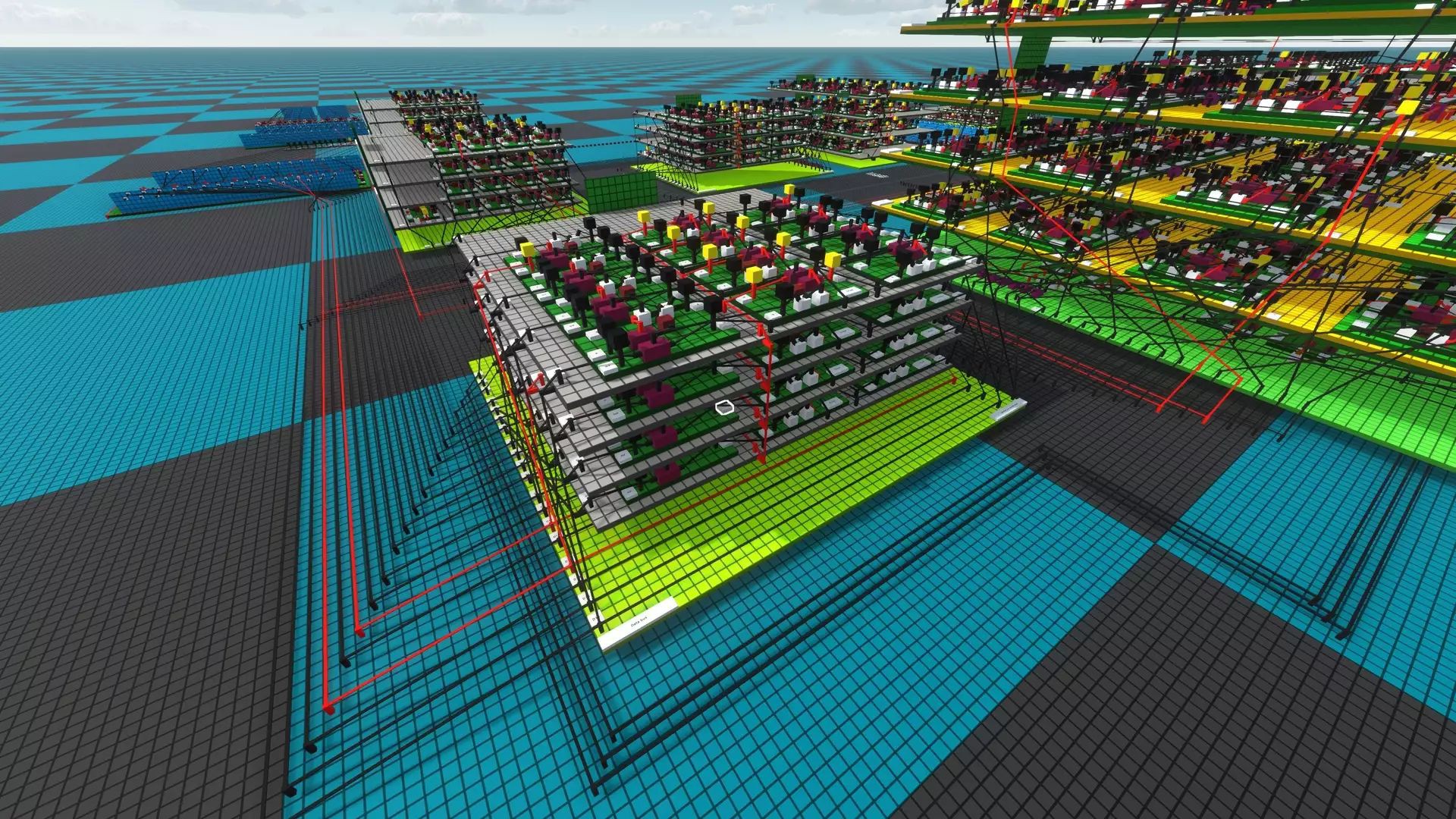
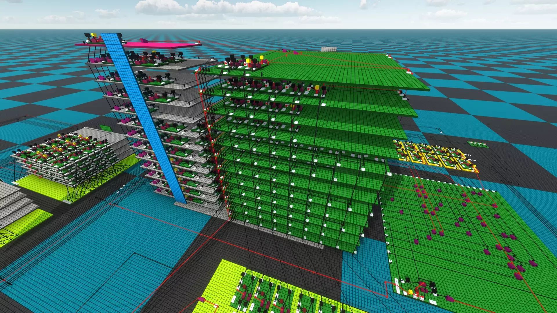
Overview 1
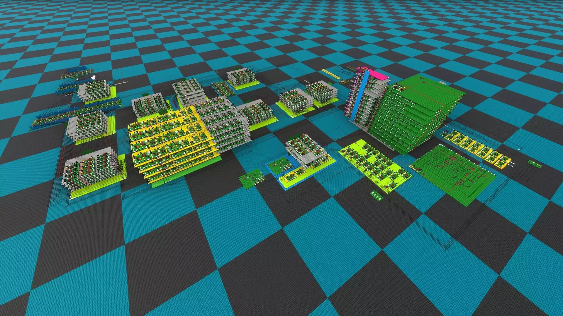
Overview 2
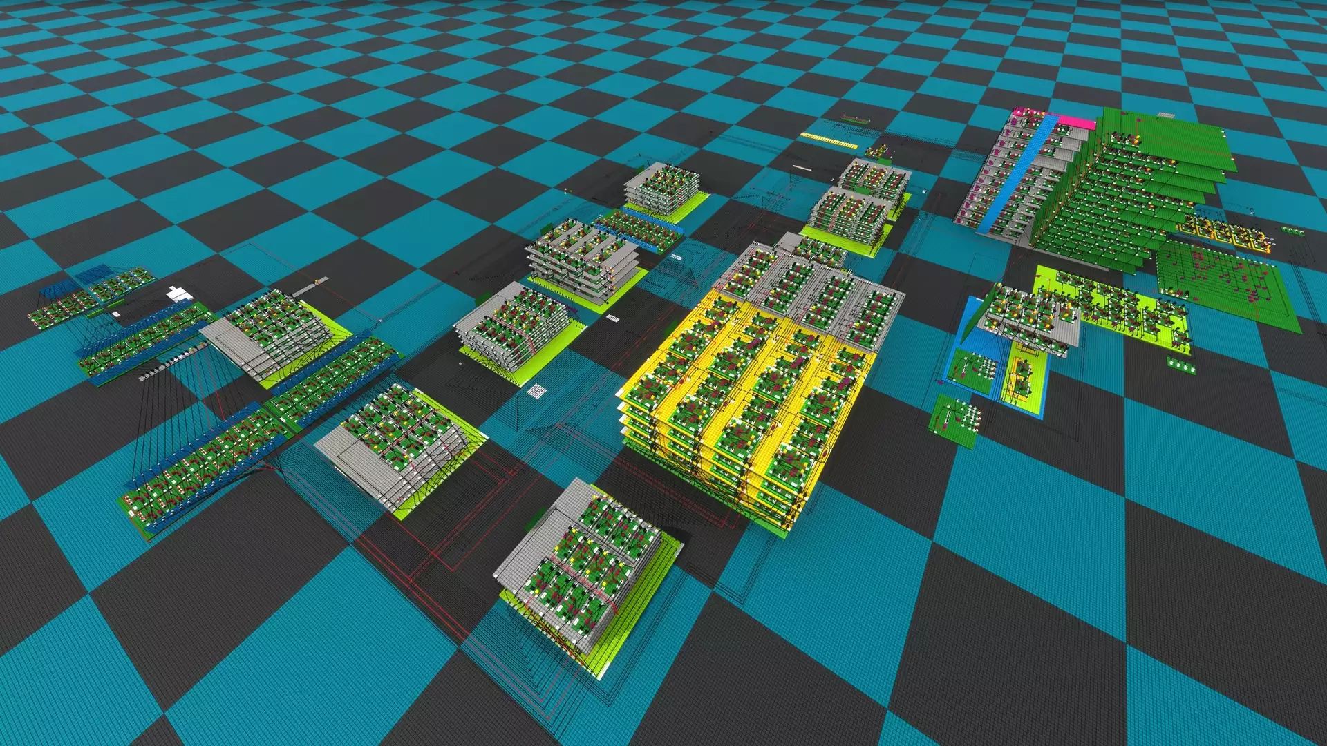
Overview 3
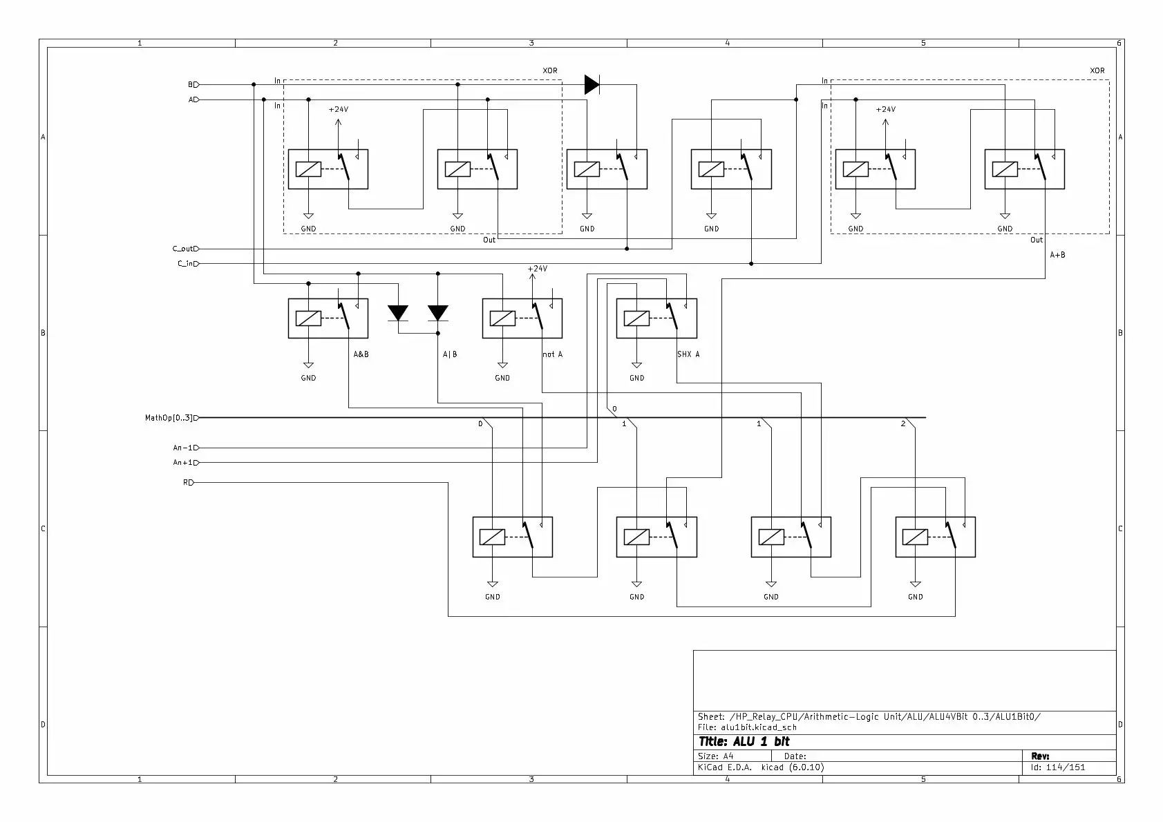
The ALU
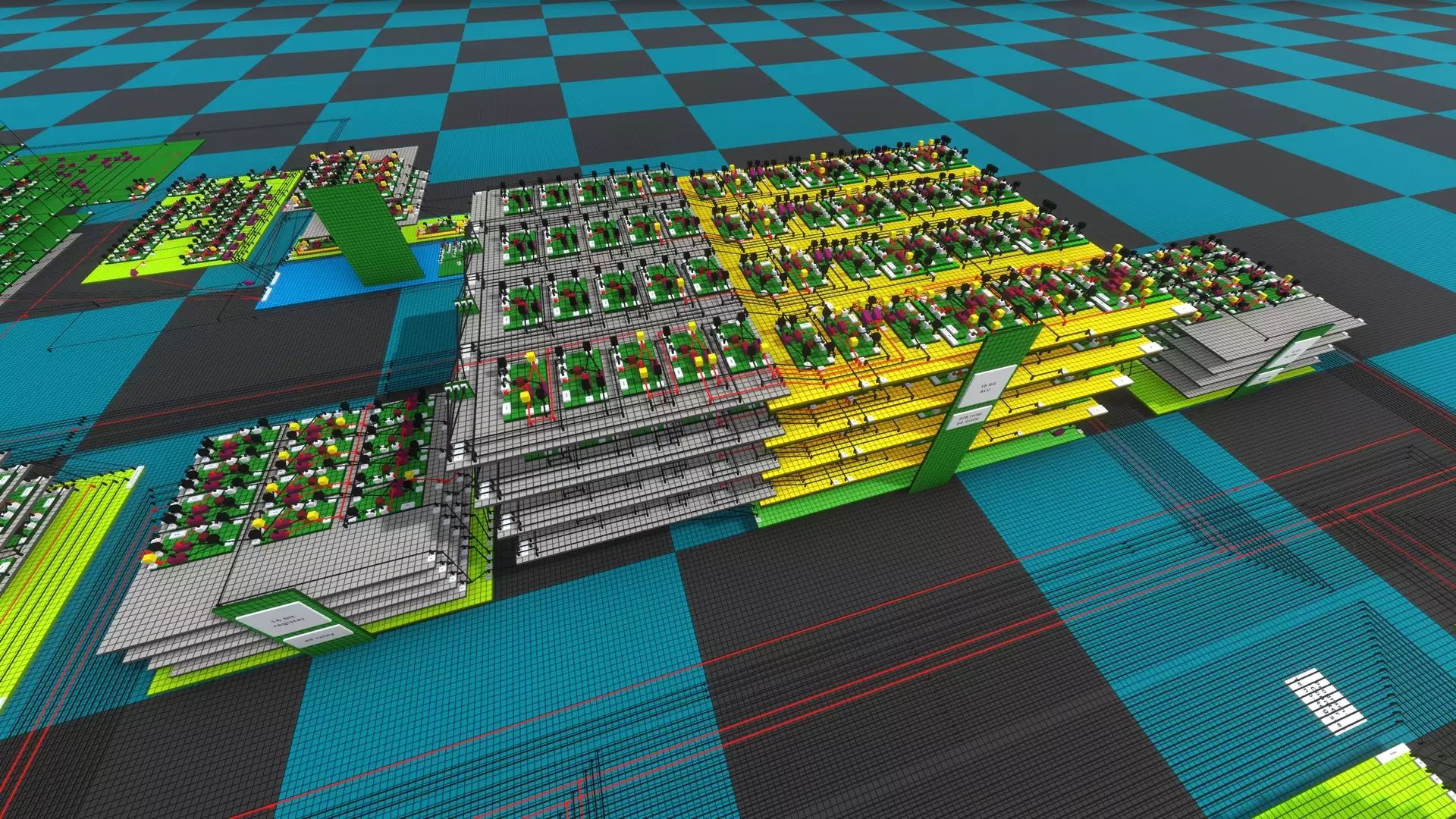
The +1 adder for the program counter
The accu
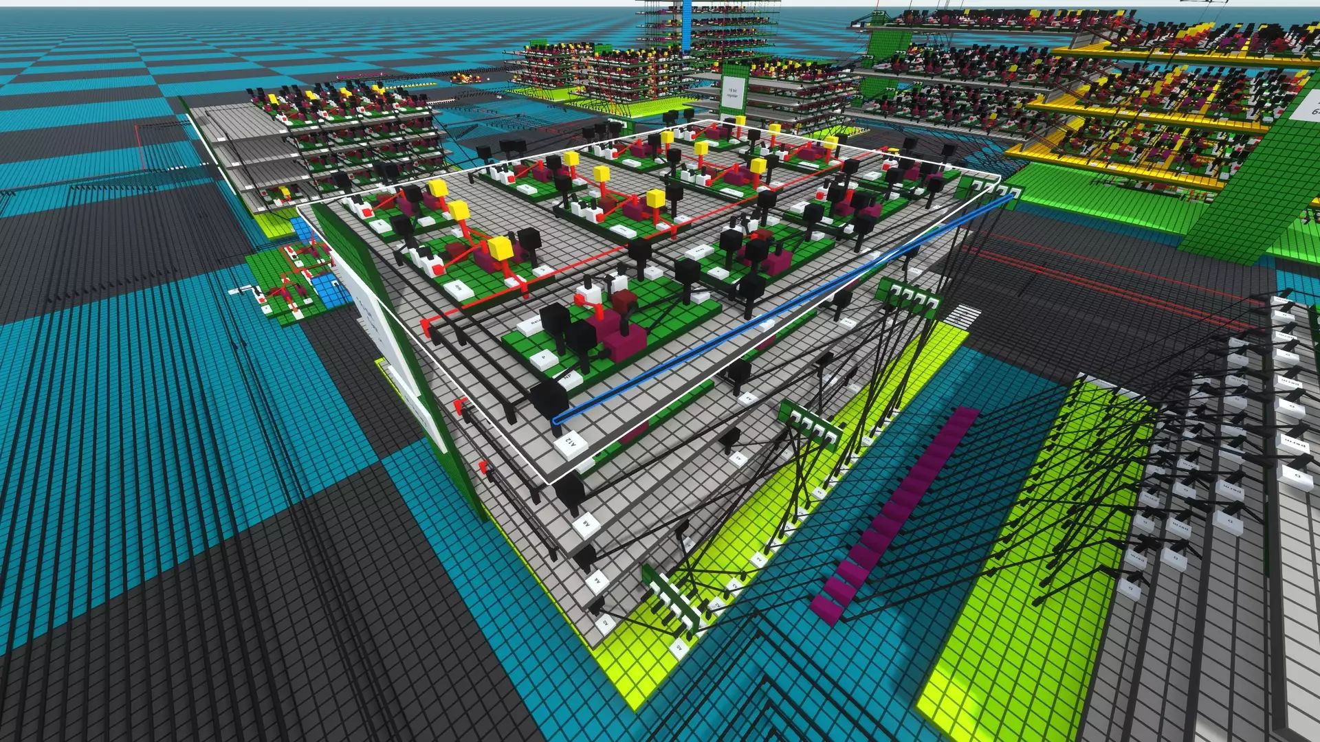
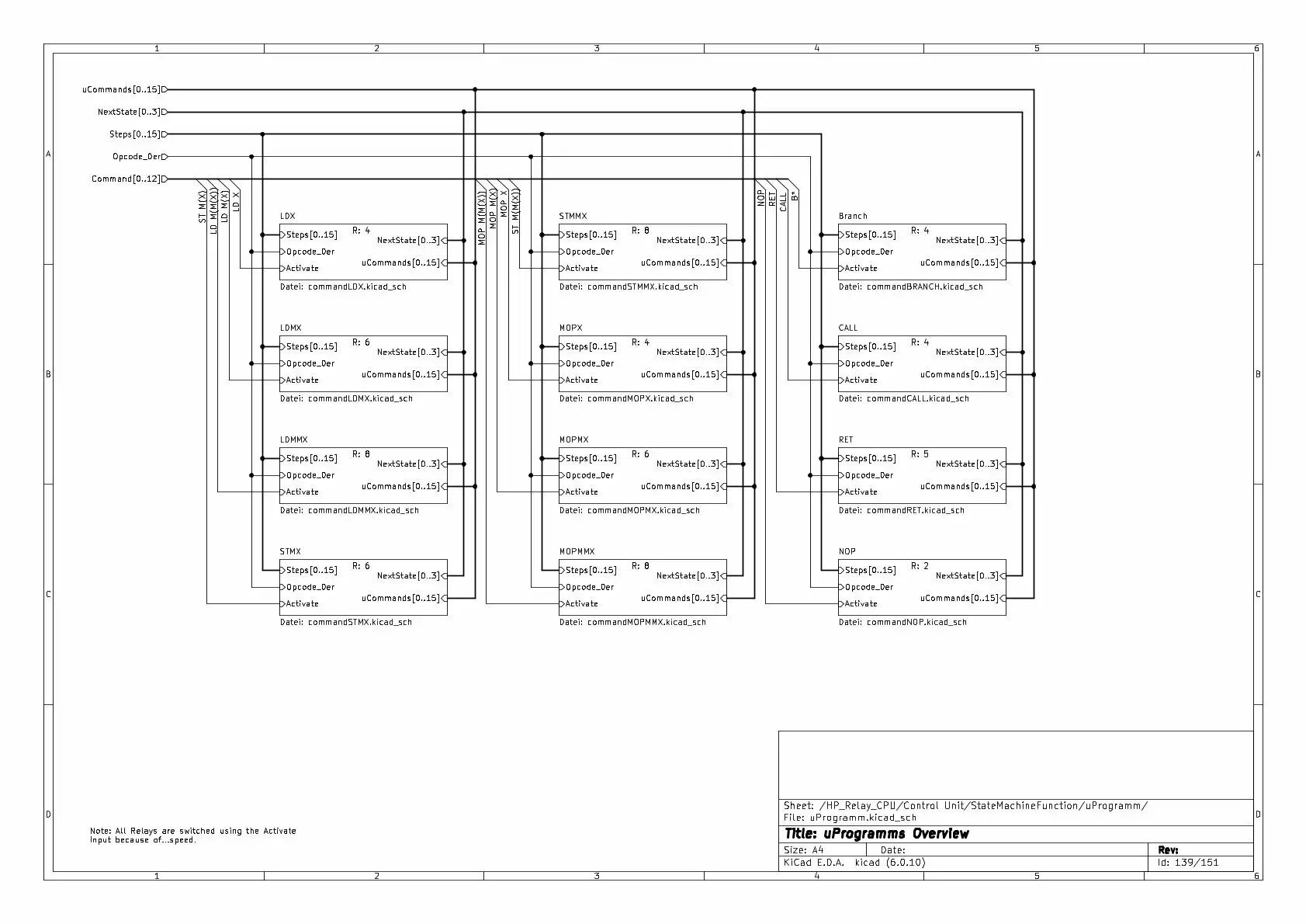
The command decoder and the state machine function
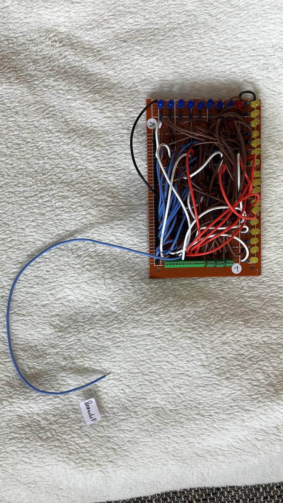
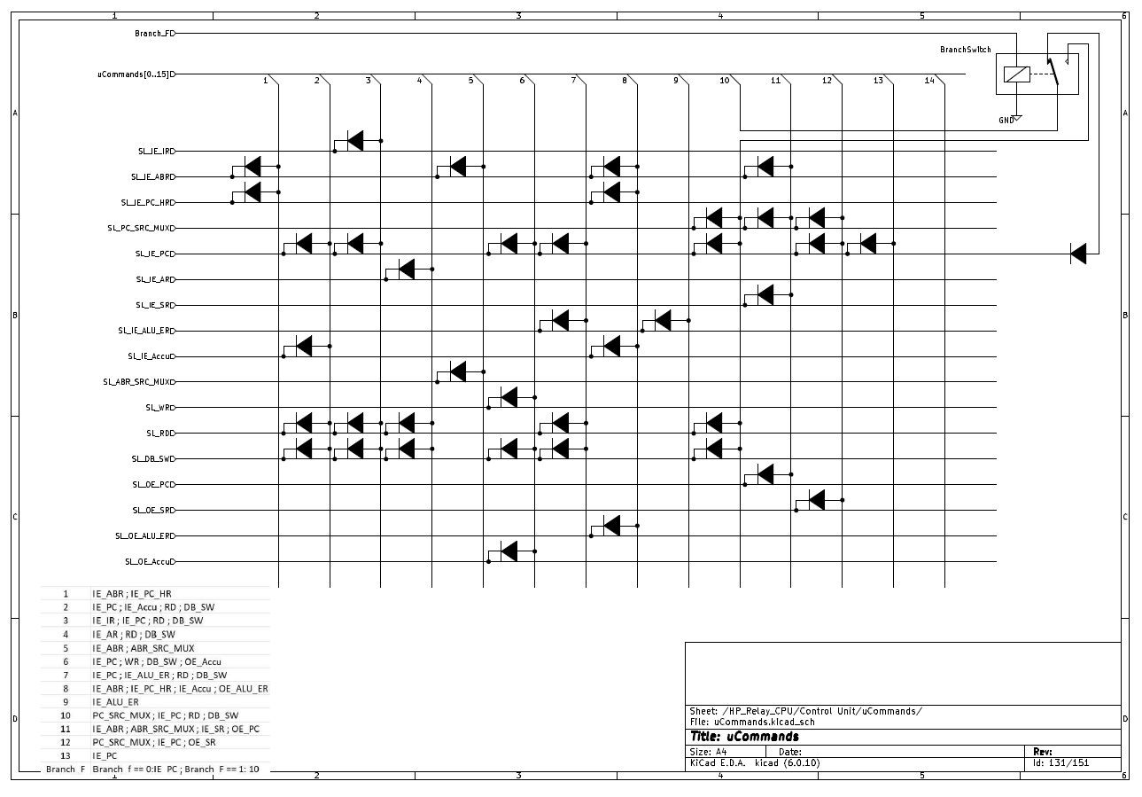
The uCommands
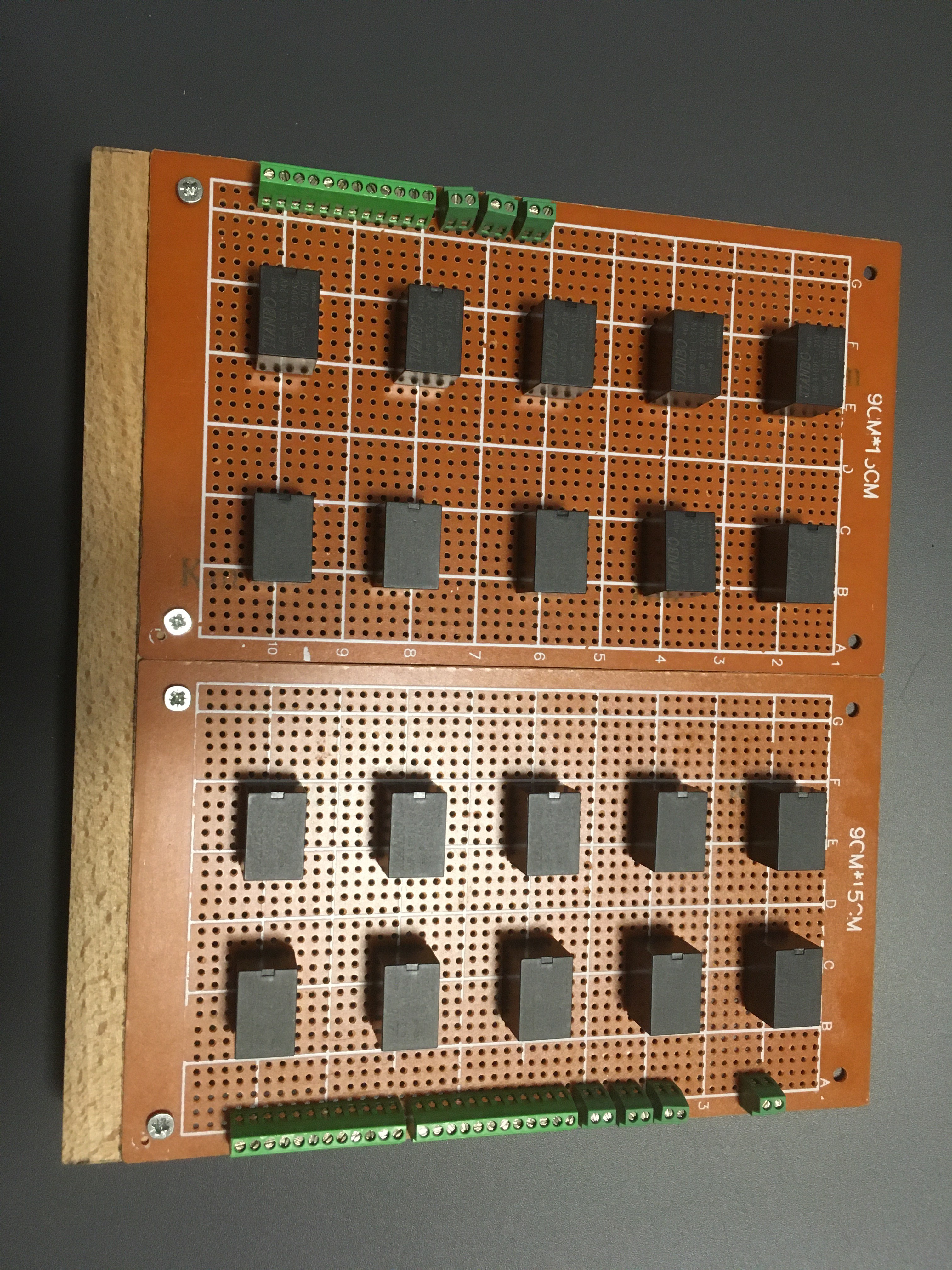
Design
One detail is important to understand the design of the system: all registers, which are realized by "self retaining" relays, have to be cleared before any information can be stored, also before the stored information can be changed. Thats the reason why the clock of the system is not an ordinary clock as you know it from digital systems. The clock of this system consists of 4 different pulses:
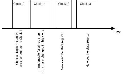
And, of course, there is not only a state register...there is also a second state register which is cleared / loaded during cycles 0 and 1. You will find this detail in the circuid diagram.
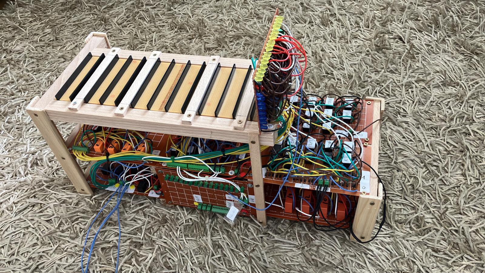
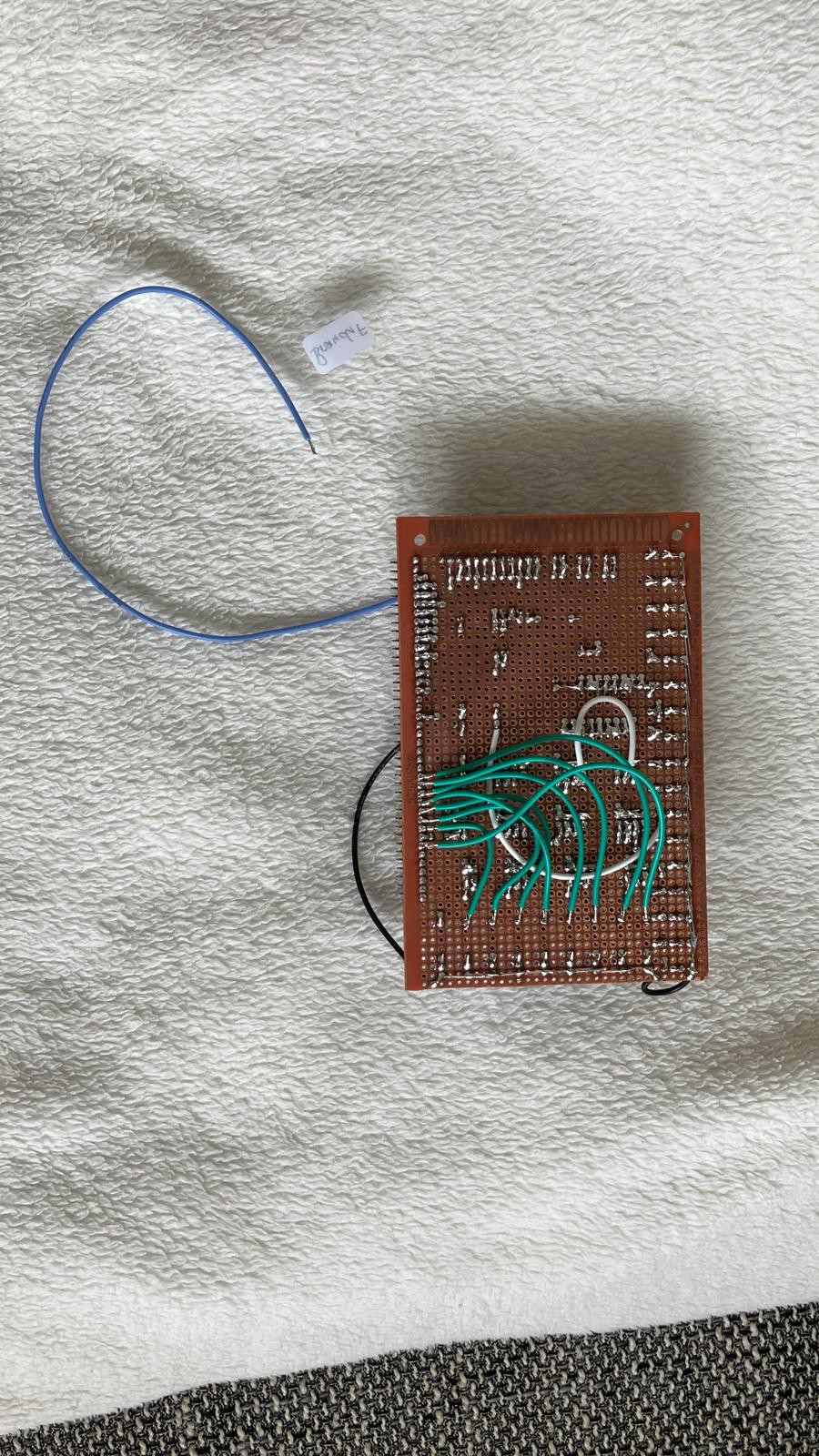
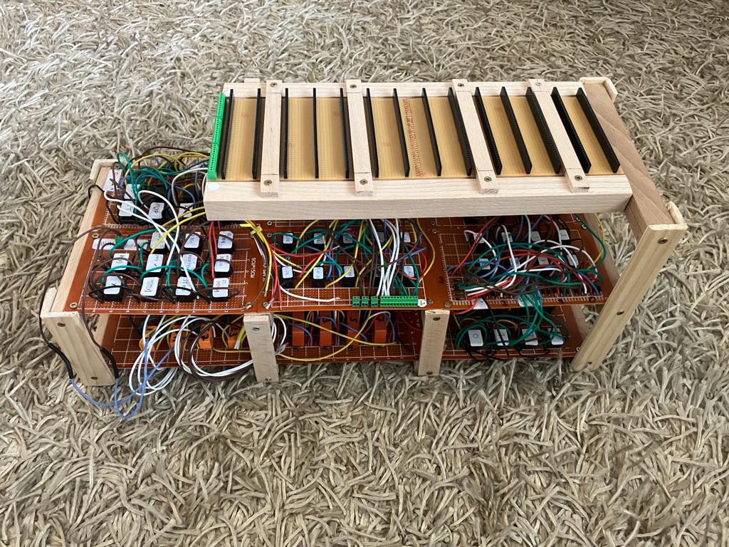
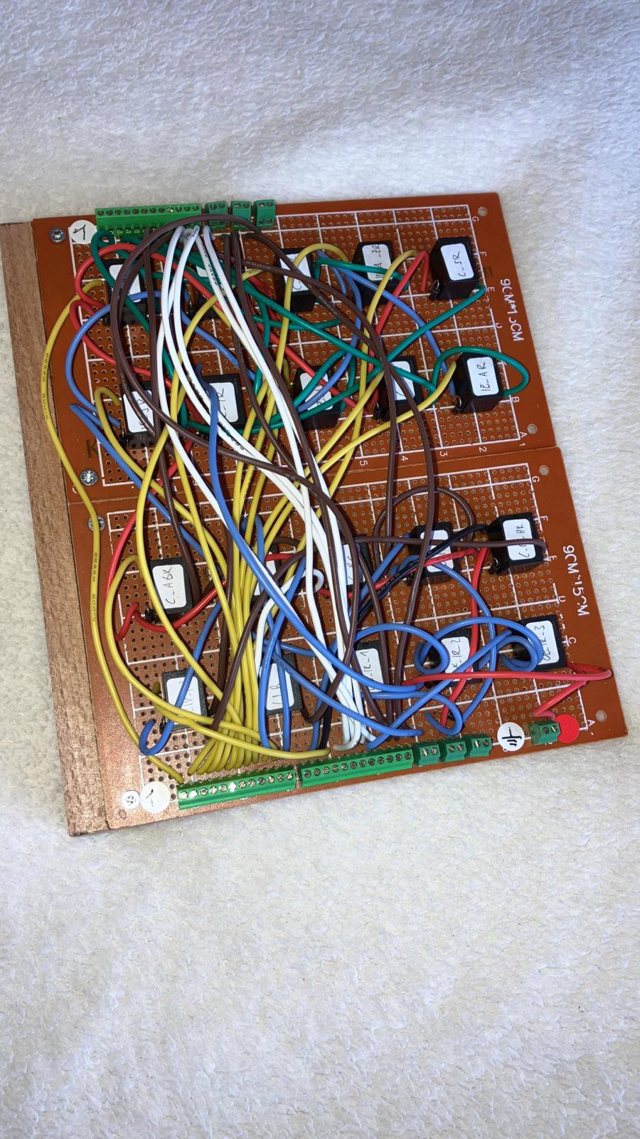
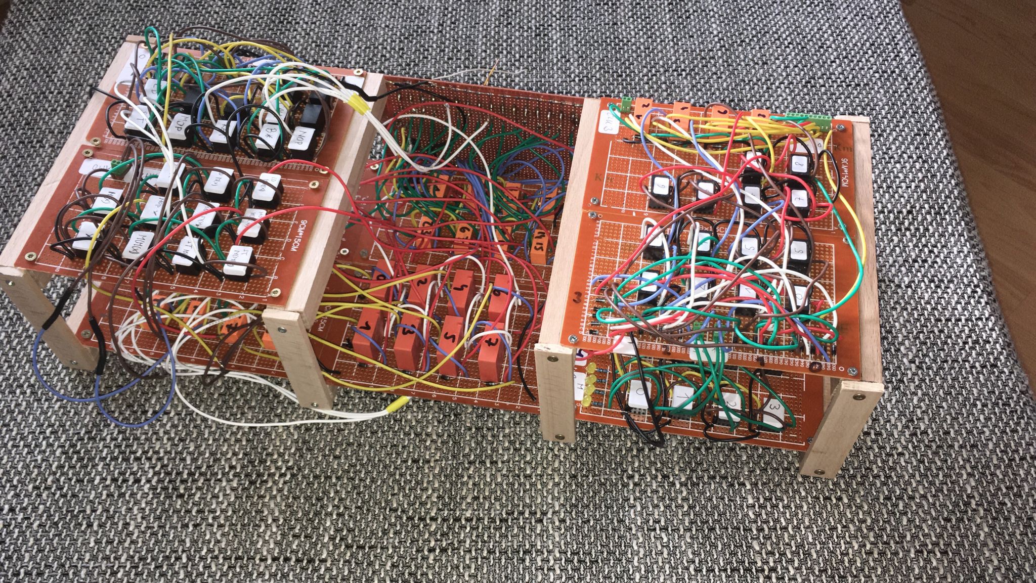
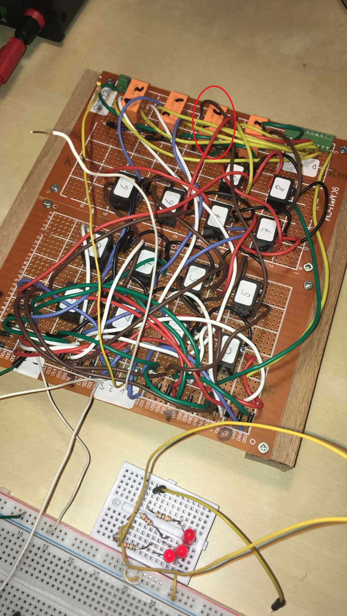
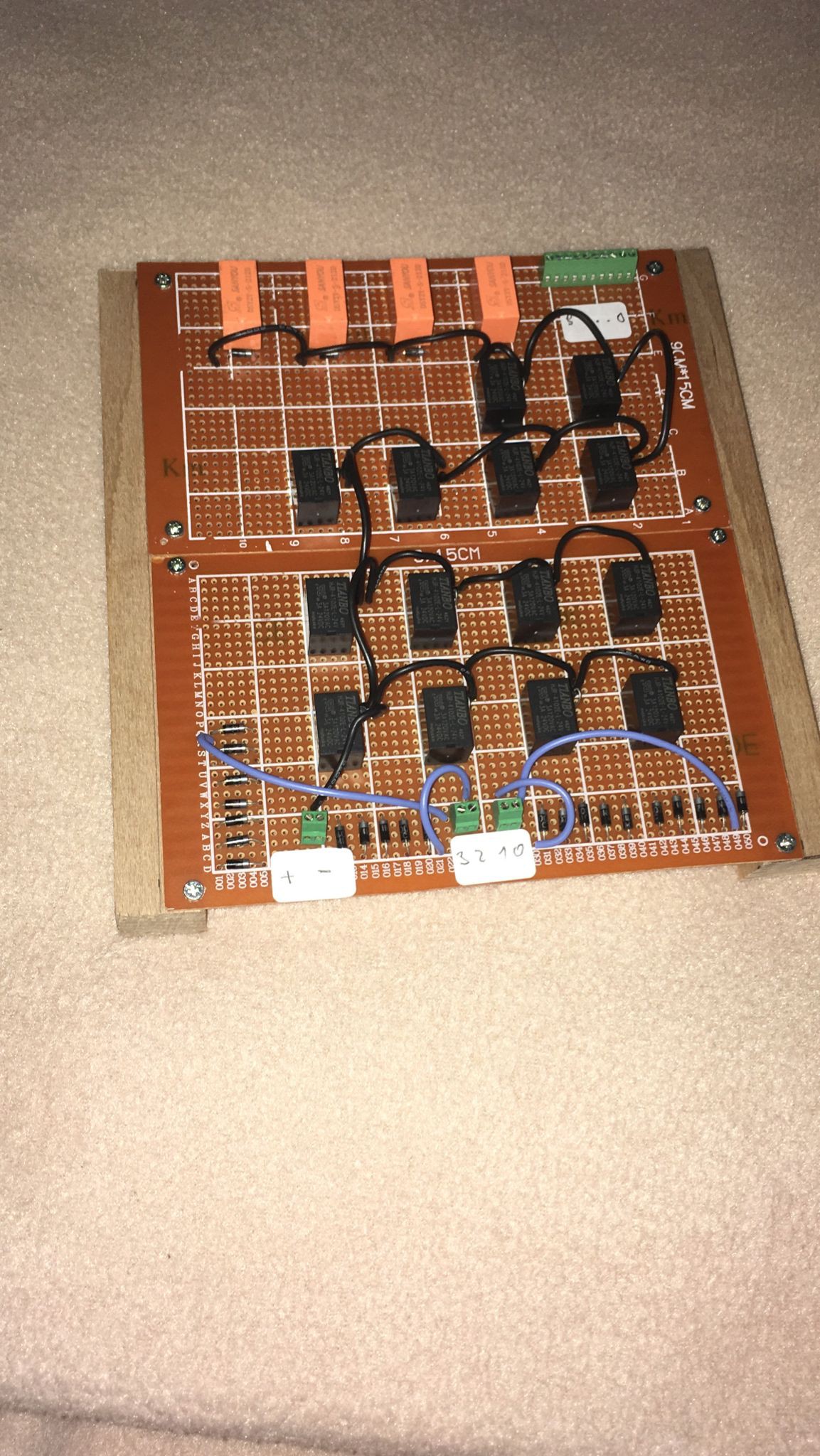
The complete system circuit diagram is avaliable in the download section. The following pitures are some key diagrams:
A system overview:
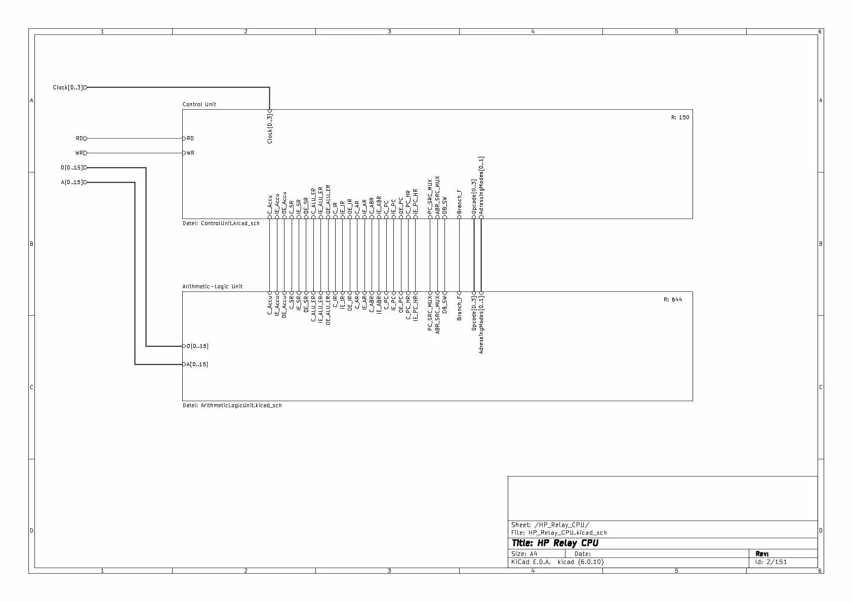
The CPU overview:
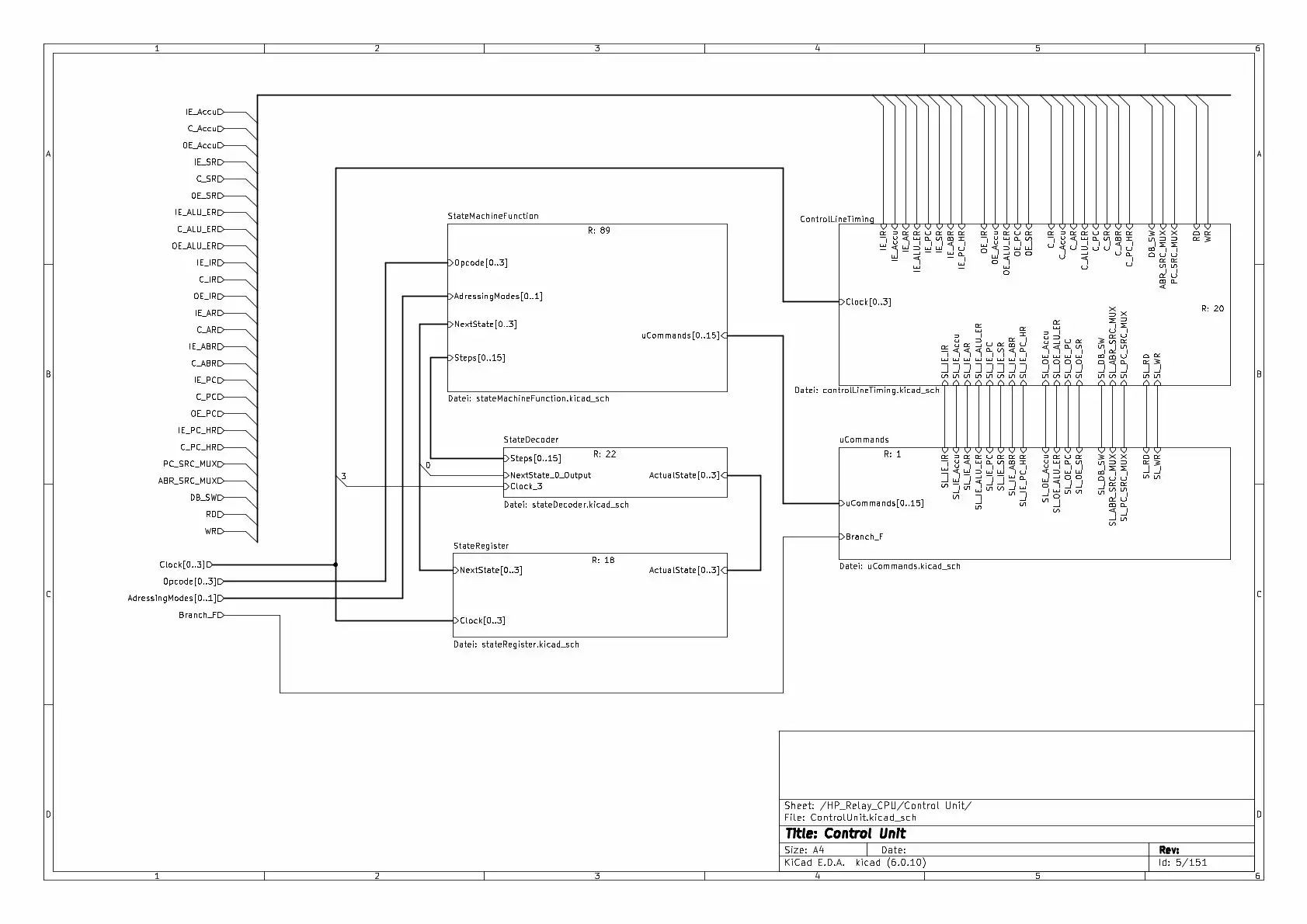
The control unit:
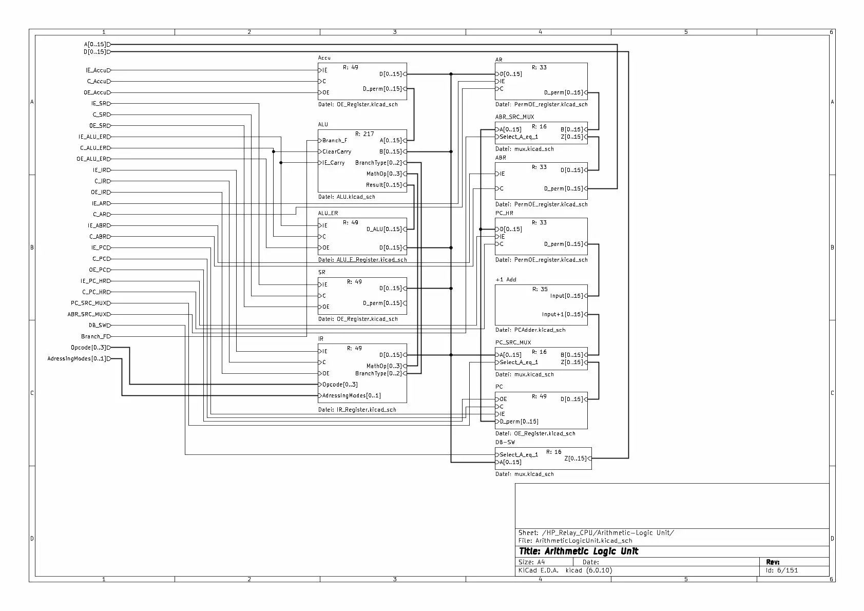
The complete ALU/register unit:
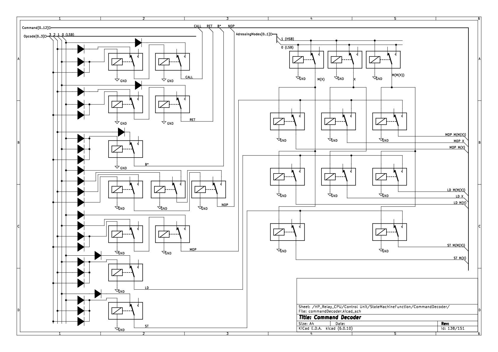
The command decoder:
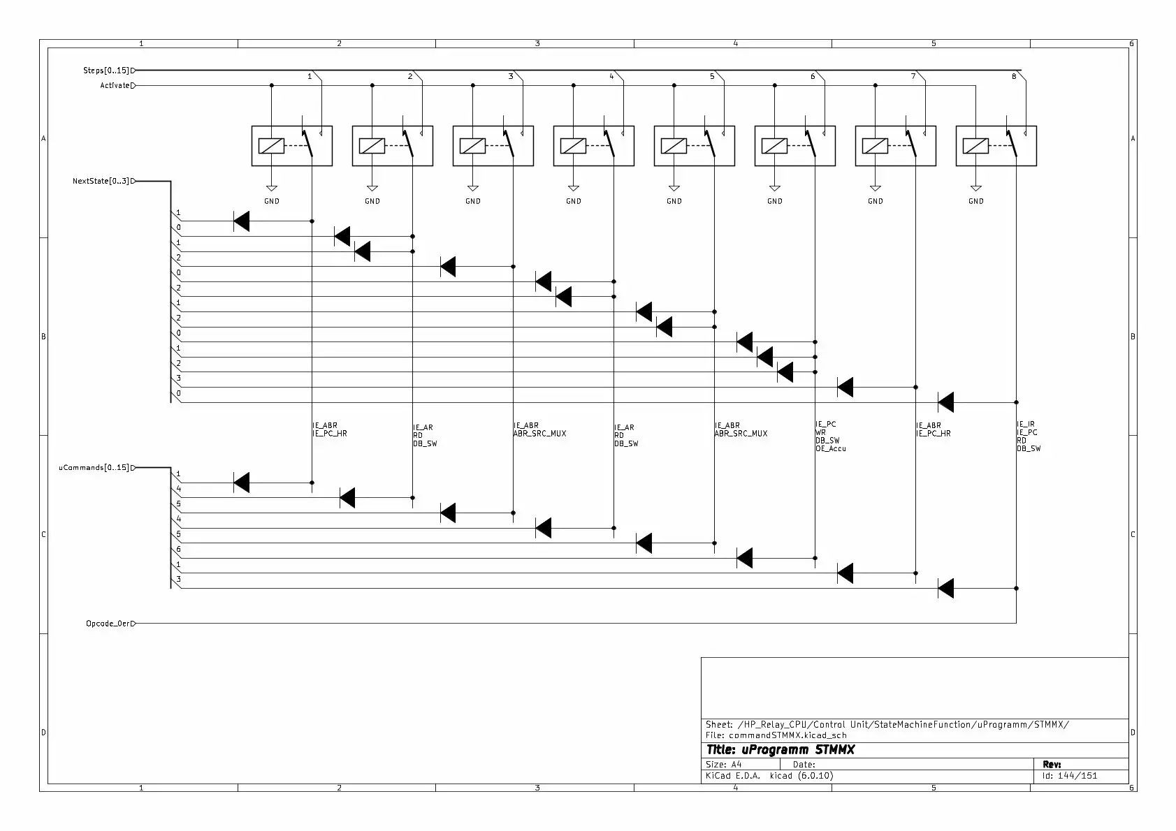
The commands state functions:
ALU operation for 1 bit:
The command state function for command ST M(M(X)):
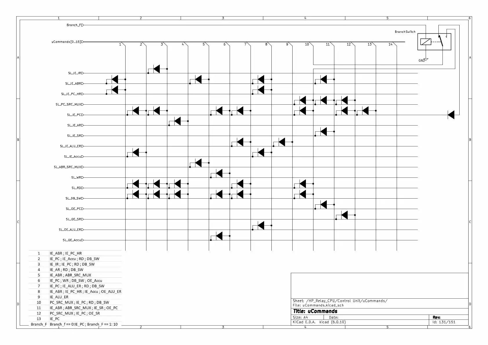
The uCommands:
The software simulation:
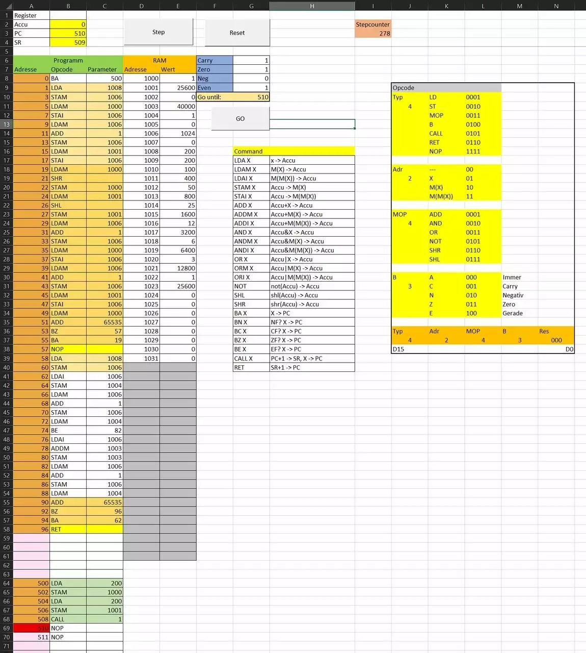
To check if the command set of the CPU is useful, a software simulation using an Excel macro was developed. Using this macro it is possible to step through the code, watch registers and memory and to go forward until a breakpoint. The following picture shows the simulation with an program which multiplies two numbers using shift operations.

 Fábio Gil
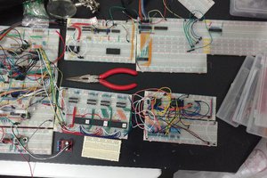
 Andre Baptista
 Dave Collins
 Artem Kashkanov