-
Normalizing LDR reading
07/01/2023 at 04:12 • 0 commentsAn LDR's resistance, RLDR can vary from about 100Ω in the sun light, to over 10MΩ in absolute darkness (source).
For practical uses we can consider one order of magnitude above and below the extremes, which in numbers means a resistance variation range from 1KΩ to 1MΩ.
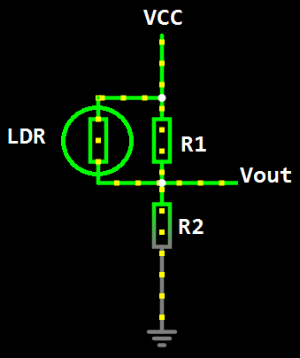
With that in mind it is possible to use the LDR along a voltage divider circuit and calculate the values of the resistors so the output voltage will match a desired range as long as such range is reasonably within the voltage rails, for instance, In a recent project I needed to use the LDR reading from an 8 bit ADC to drive a 5 bit soft PWM, then a range of 128 counts could be easily shifted right to get me the values from 0 to 31 (and avoid a floating point division math).
![]()
We have then 2 unknown variables, R1 and R2 and two known resistance values and their expected output:
- LDR in dark, R = 1MΩ, Vout = Vdark
- LDR in brightness, R = 1kΩ, Vout = Vbright
It is reasonable to consider that Vdark and Vbright will be symmetrical around Vcc/2, and to perform the calculation of the resistors we can normalize the voltage value to the resolution of the ADC (e.g. use a value of 256 in the math instead of 5V).
Rewriting the terms, considering the half of the ADC scale is 128 and half of the desired range is 64:
- LDR in dark, R = 1MΩ, ADCount = 128 + 64 = 192
- LDR in brightness, R = 1kΩ, ADCount = 128 -64 = 64
That can be solved using the voltage divider equation:
- ADCcount = ADCrange * R2 / ( R2 + R1//Rldr )
Along with the parallel resistance equation
- 1/Req = (1 / Rldr) + (1 / R1)
Combining both:
- ADCCount = ADCrange * R2 / { R2 + [ 1/ ( 1/Rldr + 1/R1 ) ] }
There are several ways to perform the math, including Wolfram Alpha, and the equation to find the resistances can be calculated using the following string
(64+128)=256*(r2)/(r2+(1/(1/1000+1/r1))); (128-64)=256*(r2)/(r2+(1/(1/1000000+1/r1)))
The calculated values will hardly be an exact value, but the E24 series can provide values close enough to get the desired counts from the ADC
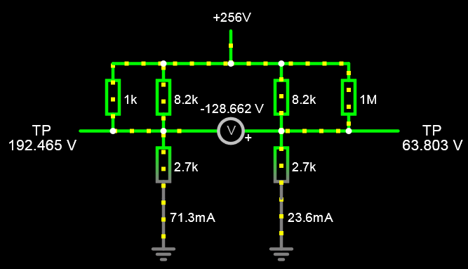
Resistor Calculated Value Closest E24 Value R1 ~8072Ω 8K2 Ω R2 ~2669Ω 2K7 Ω It is possible to use the Falstad online simulator to check how good the picked values are, and of course to fiddle with the values. To save time it is possible to use the link below the access the simulation.
INotice that the Vcc voltage was set to 256 to make it easy to check the ADC count values from the LDR in brightness (left) and in darkness (right). The difference between readings is shown in the middle. Also notice the E24 series values provided good results (no need to use precision resistors)
![]()
Epilogue:
if the LDR is exposed under extreme conditions the resistance values canreach the maximum values and the voltage range will differ from the calculated, therefore it is necessary to limit the range in software. It will also be necessary to subtract the value from the minimum expected value to have a light reading value starting from 0 (zero).
#define VMAX 192
#define VMIN 64
...
tempValue= adcRead( LDR_CHANNEL);
if (tempValue > VMAX) lightValue = VMAX;
if (tempValue < VMIN) lightValue = VMIN;
lightOutput = tempValue - VMIN;
...
In my case specifically all that's left to do to call it a day is to shift right the light output value to have the Toff within the 0-32 range.
tOFF = lightOutput >> 2;
-
Ninja Tap patch for Rock'N'Roller (MSX1)
03/17/2023 at 04:33 • 0 commentsAfter a suggestion from [gdx] from MRC I took a look at the Rock'N'Roller (MSX1) and started to work on a patch for Ninja/Shinobi Tap multi controller adapter.
![]()
First step was to disassemble the game and figure out how the game deals with the controls. There are several calls to 3 of the BIOS routines that read the keyboard, the joysticks and the trigger buttons (from the joysticks) and decided that the best strategy was to emulate such BIOS routines and return correspondent values based on the buttons pressed on the controllers plugged in the multitap adapter.
Next step was to figure out a position in RAM out of the game execution to place the patch code -> address 0xdf00 to 0xe300 seemed nice
Following I have created the alternate routines:
- ALT_SNSMAT
- ALT_GTSTCK
- ALT_GTTRIG
The alternate routines fall back to the original BIOS call when the Ninja/Shinobi tap is not detected (a flag is reset) . for instance...
ALT_GTSTCK:
    ld b,a                  ; save row number
    ld a,(ninjaDetectFlag)  ; test for ninja presence
    and a                   ;
    ld a,b                  ; restore row number
    jp z,0d5h ; (GTSTCK)    ; if not present continue with BIOS routine
    ;
    ; read and return STICK value
...
Next step was to generate a list of addresses where the BIOS calls are called and write a quick and dirt and code to replace such calls with the alternate routines created. The +1 is the offset for the instruction code CD (call) at the addresses that call the bios routines.
; Patch Original game code
    ld hl, ALT_SNSMAT  ; patch calls to 0141h (SNSMAT)
    ld (09648h+1),hl
    ld (0966bh+1),hl
    ld (09676h+1),hl
    ld (09685h+1),hl
    ld (09b7ch+1),hl
...
Then I have created a function that will be called in the game main loop to scan the joystick ports and detect the presence of a multitap adapter om port A. If an adapter is detected, a flag is marked and the four taps are read and converted as a mirror of a keyboard matrix and joystick directionals and triggers.NINJAPATCH: ; check for presence of Tap call CHECKTAPS ; c = 0 0 0 0 a1 a0 b1 b0 cpl ; c = 1 1 1 1 /a1 /a0 /b1 /b0 and 08h ; isolate bit a1 -> a = 0 0 0 0 /a1 0 0 0 ld (ninjaDetectFlag),a ; /a1 should be 1 if a ninja or shinobi is detected ret z ; scan taps ; ld de,0fa7ah ; Tap connected to joy port 2 ld de,0ba3ah ; Tap connected to joy port 1 ld hl,ntapData call GETNIN ; read TAPS on port 1 ; process taps ************************************* ...
Button Mapping
Tap 1 is mapped as :
- Up, Down, Left, Right -> Ditto
- Trigger A - Z
- Trigger B - X
- Select - SEL
- Start - Escape
That was done to allow full access and control of Options menu from the game, but it is still possible to access and control the Optiosn menu using the MSX keyboard.
Tap 2 is mapped as the QSCS (Q, S, Control, Shift) controls
Tap 3 is mapped as Joystick 1
Tap 4 is mapped as Joystick 2
To be continued... -
Keyboard Controller with Joystick for MSX (2)
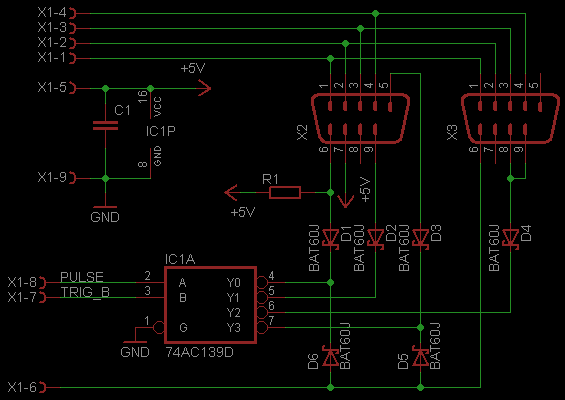
11/26/2022 at 21:33 • 0 commentsAdded a second diode to enhance the detection
![]()
And drafted some driver code that provides scan and decode that takes 98 bytes plus 5 RAM addresses.
; Scan Atari keyboard and single button joystick using
; and adapter with 74LS139

; PSG IO addresses
PSGAD: EQU 0A0H
PSGWR: EQU 0A1H
PSGRD: EQU 0A2H

; DetectKB2600 - Detect Atari controller keyboard
; Input:
;       register A: 0=Connector 1, >0=Connector 2.
; Ouptut:
;       Z -> keyboard detected
;      NZ -> keyboard adapter not detected
DetectKB2600:
  call ScanKB2600
  ld de,KBROWS
  ld c,0
Detct0:
  ld a,(de)
  and 00010000b ; isolate bit 4
  rla
  or c
  ld c,a
  inc de
djnz Detct0
  cp 01000000b
  ret

;
; ScanKB2600 - Scan Atari controller keyboard
;
; Inputs:
;        register A: 0=Connector 1, >0=Connector 2.
; Ouptuts   :          bit  7  6  5  4  3  2  1  0
;           KBROWS     ->   1  1  1  0  #  9  6  3
;           KBROWS + 1 ->   1  1  1  1  0  8  5  2
;           KBROWS + 2 ->   1  1  1  0  *  7  4  1
;(JOYTBITS) KBROWS + 3 ->   1  1  1  TA RG LF DW UP

ScanKB2600:
   ; set zero flag according to port option
   and a
   ; Save PSG Context
   ld a,15
   out (PSGAD),a
   in a,(PSGRD)
   ld (SAVPSG),a
   ld hl, KBROWS

   ; Select Joystick port accordingly
   jr NZ, ScanCon2

ScanCon1:
   and 10101101b  ; clear bit 6 -> Joysel -> joy port 0, 4:PULSE and 1:TRIGGER B
;  a = pins 8,7 low  (row 0)
   ld b,a  ; a = pin 8=0, pin 7=0 (row 0)
   set 4,b ; b = pin 8=1, pin 7=0 (row 1)
   ld c,b  ;
   set 1,c ; c = pin 8=1, pin 7=1 (row 2)
   ld d,a  ; a = pin 8=0, pin 7=0 (row 0)
   set 1,d ; b = pin 8=0, pin 7=1 (Joystick)

   jr ScanRow0

ScanCon2:

   and 10010111b  ; clear bit 5:PULSE and 3:TRIGGER B
   set 6,a        ; Set bit 6 -> Joysel -> joy port 1
   ld b,a  ; a = pin 8=0, pin 7=0 (row 0)
   set 5,b ; b = pin 8=1, pin 7=0 (row 1)
   ld c,b  ;
   set 3,c ; c = pin 8=1, pin 7=1 (row 2)
   ld d,a  ; a = pin 8=0, pin 7=0 (row 0)
   set 3,d ; b = pin 8=0, pin 7=1 (Joystick)

ScanRow0:
   ld e,a
   call SaveRow

ScanRow1:
   ld e,b
   call SaveRow

ScanRow2:
   ld e,c
   call SaveRow

ScanJoy:
   ld e,d
   call SaveRow

RestorePSG:
   ld e,(hl) ; hl now points to SAVPSG

SaveRow:
   di             ; disable interrupts
   ld a,15
   out (PSGAD),a
   ld a, e
   out (PSGWR),a  ; update register 15
   ld a,14
   out (PSGAD),a  ; select register 14
   in a,(PSGRD)   ; read keys hhhh*741
   or 11110000b   ; mask unused bits
   ld (HL),a      ; save keyboard state
   inc hl
   ei
   ret

 ; Variables
; keyboard rows HHHL#963, HHHH0852, HHHL*741
 KBROWS:  DS 3
 JOYBITS: DS 1
;   PSG register 15 save state during execution, destroyed buttons at the end
; must be contiguous to Joybits
 SAVPSG: DS 1
My Projects
My Pages
Things I've Built
Chez Le Chien
Apartment Houses for my Dachshunds
Sensor Shield
Arduino Shield for interaction with MIT's Scratch. Provides the same functionality of PicoBoard
Nunchucks for Atari
Adapter board for playing Atari games with a Nunchuck controller. Based on a PIC micro.
Nunchuck in MSX
Nunchuck Adapter for MSX computers using bitbanged I2C directly on the Joystick port
Projects I Like & Follow
Share this profile
ShareBits
Become a Hackaday.io Member
Create an account to leave a comment. Already have an account? Log In.
Salve Flames! Esse projeto é bem da hora mesmo!
Grande abraço!!!
Thanks for liking #Restoring a Beckman neon display clock !
Just based on the other projects you follow – let alone your own excellent projects – I'm honored that you would follow my humble keyboard hack! Thanks!
I also echo tyler's comment below about your tag-line.
Thanks for your interest in my 2:5 Scale KENBAK-1 Personal Computer Reproduction and Sol-20 Reproduction projects.
Thank you for liking my #CRISS CP/M 8-bit Homebrew DIY Computer (AVR based) project!
Thanks, cool cat @danjovic for liking #6 segments suffice and #TTL binary clock !
Thank you for your interest in my 2:3 Scale VT100 Terminal Reproduction project.
Hello again and thank you for liking my #how I make masks project! :)
Hello and thank you for liking my #practice backpack project!
Good morning once again and thank you for liking my #LLTP - Light Logic Transistorless Processor
Good morning and once again, thanks for the like, this time for #Shortwave Crystal Radio - A blast from my past.
Hi Danjovic, thanks for liking the #Kobold K2 - RISC TTL Computer !
Hello Danjovic, thank you for liking my Clock, the 1 Square Inch TTL CPU , the #4 bit TTL ALU and the #Handheld 3GHz Spectrum Analyzer !


 danjovic


 mircemk
 bobricius
 Don
Don Augusto Baffa
 Dr. Cockroach
 Ted Fried
 Moritz v. Sivers
 Nicola Cimmino
 Turi
Turi Keith
Keith Stefan Wagner
 davedarko
 Denver


Salve Mestre, dá uma olhada nesse projeto. Bem legal.
RetroVGA - Raspbery Pico multi retro computer | Hackaday.io